Features: Member of the Texas Instruments
Widebus(TM) Family EPIC (TM) (Enhanced-Performance Implanted
CMOS) Submicron Process Typical VOLP (Output Ground Bounce)
< 0.8 V at Vcc = 3.3 V, TA = 25
Typical VOHV (Output VOH Undershoot)
> 2 V at VCC = 3.3 V, TA = 25
Latch-Up Performance Exceeds 250 mA
Per JEDEC Standard JESD-17 Bus Hold on Data Inputs Eliminates the
Need for External Pullup/Pulldown
Resistors Package Options Include Plastic 300-mil
Shrink Small-Outline (DL) and Thin Shrink
Small-Outline (DGG) Packages
Pinout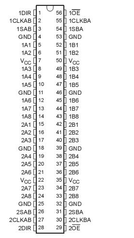 SpecificationsSupply voltage range, VCC . . . . . . . . . . . . . . . . . . . . . . . . . . . . . . . . . . . . . . . . . . . . . . . . . . . 0.5 V to 4.6 V
Input voltage range, V I: Except I/O ports (see Note 1) . . . . . . . . . . . . . . . . . . . . . . . . . . . . . 0.5 V to 4.6 V
I/O ports (see Notes 1 and 2) . . . . . . . . . . . . . . . . . . . . ................................... . . . . . 0.5 V to VCC + 0.5 V
Output voltage range, VO (see Notes 1 and 2) . . . . . . . . . . . . . . . . . . . . . . . . . . . . . 0.5 V to VCC + 0.5 V
Input clamp current, IIK (V I < 0) . . . . . . . . . . . . . . . . . . . . . . . . . . . . . . . . . . . . . . . . . . . . . . . . . . . 50 mA
Output clamp current, IOK (VO < 0 or V O > VCC ) . . . . . . . . . . . . . . . . . . . . . . . . . . . . . . . . . . . . . ± 50 mA
Continuous output current, IO (VO = 0 to VCC ) . . . . . . . . . . . . . . . . . . . . . . . . . . . . . . . . . . . . . . . . ± 50 mA
Continuous current through VCC or GND . . . . . . . . . . . . . . . . . . . . . . . . . . . . . . . . . . . . . . . . .. . ... . ±100 mA
Maximum power dissipation at T A = 55 (in still air) (see Note 3): DGG package . . . . . . . . . . . . . . .. . . . 1 W
DL package . . . . . . . . . . . . . . . . . . 1.4 W
Storage temperature range, Tstg. . . . . . . . . . . . . . . . . . . . . . . . . . . . . . . . . . . . . . . . . . . . . . . .65 to 150
DescriptionThis 16-bit bus transceiver and register is designed for low-voltage (3.3-V) VCC operation. The SN74LVC16646 can be used as two 8-bit transceivers or one 16-bit transceiver. The device
consists of bus transceiver circuits, D-type flip-flops, and control circuitry arranged for multiplexed transmission of data directly from the input bus or from the internal registers. Data on the A or B bus is clocked into the registers on the low-to-high transition of the appropriate clock (CLKAB or CLKBA) input. Figure 1 illustrates the four fundamental bus-management functions that can be performed with the SN74LVC16646.
SN74LVC16646 Output-enable (OE) and direction-control (DIR) inputs control the transceiver functions. In the transceiver mode, data present at the high-impedance port may be stored in either register or in both. The select-control (SAB and SBA) inputs can multiplex stored and real-time (transparent mode) data. The circuitry used for select control eliminates the typical decoding glitch that occurs in a multiplexer during the transition between stored and real-time data. DIR determines which bus receives data when OE is low. In the isolation mode (OE high), A data may be stored in one register and/or B data may be stored in the other register.
When an output function is disabled, the SN74LVC16646 input function is still enabled and can be used to store and transmit data. Only one of the two buses, A or B, may be driven at a time.
To ensure the high-impedance state during power up or power down, SN74LVC16646 OEshould be tied to VCC through a pullup resistor; the minimum value of the resistor is determined by the current-sinking capability of the driver.
Active bus-hold circuitry holds unused or floating data inputs at a valid logic level.
The SN74LVC16646 is characterized for operation from 40°C to 85°C.

 SN74LVC16646 Data Sheet


