Features: Members of the Texas Instruments Widebus(TM) Family
State-of-the-Art Advanced BiCMOS
Technology (ABT) Design for 3.3-V Operation and Low Static-Power Dissipation
Support Mixed-Mode Signal Operation (5-V Input and Output Voltages With 3.3-V V ) CC
Support Unregulated Battery Operation Down to 2.7 V
Typical V (Output Ground Bounce) OLP <0.8 V at V = 3.3 V, T = 25 C CC A °
I off and Power-Up 3-State Support Hot Insertion
Distributed V and GND Pins Minimize CC
High-Speed Switching Noise
Flow-Through Architecture Optimizes PCB
Layout Latch-Up Performance Exceeds 100 mA Per JESD 78, Class
II ESD Protection Exceeds JESD 22
2000-V Human-Body Model (A114-A)
200-V Machine Model (A115-A)
1000-V Charged-Device Model (C101) Package Options Include
Plastic Shrink Small-Outline (DL) and Thin Shrink Small-Outline (DGG) Packages and 380-mil Fine-Pitch Ceramic Flat (WD) Package Using 25-mil Center-to-Center SpacingsPinout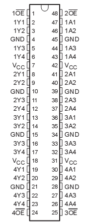 SpecificationsSupply voltage range, V . . . . . . . . . . . . . . . . . . . . . . . . . . . . . . . . . . . . . . . . . . . . . 0.5 V to 4.6 VCC
Input voltage range, V (see Note 1) . . . . . . . . . . . . . . . . . . . . . . . . . . . . . . . . . . . . . . 0.5 V to 7 VI
Voltage range applied to any output in the high-impedance
or power-off state, V (see Note 1) . . . . . . . . . . . . . . . . . . . . . . . . . . . . . . . . . . . ..... . 0.5 V to 7 VO
Voltage range applied to any output in the high state, V (see Note 1) . . . . 0.5 V to V + 0.5 VO CC
Current into any output in the low state, I : SN54LVT16240 96 mA. . . . . . . . . . . . . . . . . . . . .. . . . . . O
Current into any output in the high state, I (see Note 2): SN54LVT16240 . . . . . . . . . ... . . . . 48 mAO
Input clamp current, I (V < 0) . . . . . . . . . . . . . . . . . . . . . . . . . . . . . . . . . . . . . . . . . . . . . . 50 mAIK I
Output clamp current, I (V < 0) . . . . . . . . . . . . . . . . . . . . . . . . . . . . . . . . . . . . . . . . . . . . 50 mA OK O
Package thermal impedance, q JA (see Note 3): DGG package . . . . . . . . . . . . . . . . . . . . . . . . 70°C/W
DL package . . . . . . . . . . . . . . . . . . . . . . ......................................................................... . . . . . 63°C/W
Storage temperature range, T 65. . . . . . . . . . . . . . . . . . . . . . . . . . . . . . ............ . . . . . . . C to 150 C
DescriptionThe SN74LVT16240 devices are 16-bit buffers and line drivers designed specifically for low-voltage (3.3-V) V
CC operation, but with the capability to provide a TTL interface to a 5-V system environment.
These devices SN74LVT16240 are designed specifically to improve both the performance and density of 3-state memory address drivers, clock drivers, and bus-oriented receivers and transmitters.
The devices SN74LVT16240 can be used as four 4-bit buffers, two 8-bit buffers, or one 16-bit buffer. The devices provide inverting outputs and symmetrical active-low output-enable (OE) inputs.When V is between 0 and 1.5 V, the devices are in the high-impedance state during power up or power down.
CC However, to ensure the high-impedance state above 1.5 V, OE should be tied to V through a pullup resistor;
CC the minimum value of the resistor is determined by the current-sinking capability of the driver.

 SN74LVT16240 Data Sheet


