ApplicationAudio www.ti.com/audio
Automotive www.ti.com/automotive
Broadband www.ti.com/broadband
Digital Control www.ti.com/digitalcontrol
Military www.ti.com/military
Optical Networking www.ti.com/opticalnetwork
Security www.ti.com/security
Telephony www.ti.com/telephony
Video & Imaging www.ti.com/video
Wireless www.ti.com/wireless
Pinout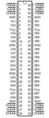 Specifications
Supply voltage range, VCC . . . . . . . . . . . . . . . . . . . . . . . . . . . . . . . . . . . . . . . . 0.5 V to 4.6 V
Input voltage range, VI (see Note 1) . . . . . . . . . . . . . . . . . . . . . . . . .. . . . . . . . . . 0.5 V to 7 V
Voltage range applied to any output in the high-impedance
or power-off state, VO (see Note 1) . . . . . . . . . . . . . . . . . . .. . . . . . . . . . . . . . . . . 0.5 V to 7 V
Voltage range applied to any output in the high state, VO (see Note 1) .0.5 V to VCC + 0.5 V
Current into any output in the low state, IO: SN54LVTH16543 . . . . . . . . . . . . . . . . . . . . . 96 mA
SN74LVTH16543 . . . . . . . . . . . . . . . . . . . 128 mA
Current into any output in the high state, IO (see Note 2): SN54LVTH16543 . . . . . . . . . . 48 mA
SN74LVTH16543 . . . . . .. . . . . 64 mA
Input clamp current, IIK (VI < 0) . . . . . . . . . . . . . . . . . . . . . . . . . . . . . . . . . . . . . . . . . . . . 50 mA
Output clamp current, IOK (VO < 0) . . . . . . . . . . . . . . . . . . . . . . . . . . . . . . . . . . . . . . . . . 50 mA
Package thermal impedance, qJA (see Note 3): DGG package . . . . . . . . . . . . . . . . . . . . . 89°C/W
DL package . . . . . . . . . . . . . . . . . . . . . . . 94°C/W
Storage temperature range, Tstg . . . . . . . . . . . . . . . . . . . . . .. . . . . . . . . . . . . . . 65°C to 150°C
† Stresses beyond those listed under "absolute maximum ratings" may cause permanent damage to the device. These are stress ratings only, and functional operation of the device at these or any other conditions beyond those indicated under "recommended operating conditions" is not implied. Exposure to absolute-maximum-rated conditions for extended periods may affect device reliability.
NOTES: 1. The input and output negative-voltage ratings may be exceeded if the input and output clamp-current ratings are observed.
2. This current flows only when the output is in the high state and VO > VCC.
3. The package thermal impedance is calculated in accordance with JESD 51.
DescriptionThe SN74LVTH16543 devices are 16-bit registered transceivers designed for low-voltage (3.3-V) VCC operation, but with the capability to provide a TTL interface to a 5-V system environment. These devices can be used as two 8-bit transceivers or one 16-bit transceiver. Separate latch-enable (LEAB or LEBA) and output-enable (OEAB or OEBA) inputs are provided for each register to permit independent control in either direction of data flow.
About SN74LVTH16543,The A-to-B enable (CEAB) input must be low to enter data from A or to output data from B. If CEAB is low and LEAB is low, the A-to-B latches are transparent; a subsequent low-to-high transition of LEAB puts the A latches in the storage mode. With CEAB and OEAB both low, the 3-state B outputs are active and reflect the data present at the output of the A latches. Data flow from B to A is similar but requires using the CEBA, LEBA, and OEBA inputs.

 SN74LVTH16543 Data Sheet


