SN75LVDT1422

Features: · 10 MHz to 100 MHz Shift Clock Support · 175 Mbytes/sec In TX/RX Modes · Reduces Cable Size, Cost, and System EMI· Bidirectional Data Communication· Total Power < 360 mW Typ at 100-MHz Worst Case Pattern· Power-Down Mode: < 500 µW Typ· No External Components Required for PLL...

product image

SN75LVDT1422 Picture
SeekIC No. : 004499791 Detail

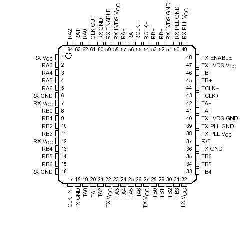
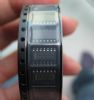
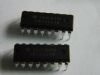
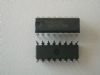
SN75LVDT1422: Features: · 10 MHz to 100 MHz Shift Clock Support · 175 Mbytes/sec In TX/RX Modes · Reduces Cable Size, Cost, and System EMI· Bidirectional Data Communication· Total Power < 360 mW Typ at 100-MHz...

floor Price/Ceiling Price

Part Number:
SN75LVDT1422
Supply Ability:
5000

Price Break

  • Qty
  • 1~5000
  • Unit Price
  • Negotiable
  • Processing time
  • 15 Days
Total Cost: $ 0.00

SeekIC Buyer Protection PLUS - newly updated for 2013!

  • Escrow Protection.
  • Guaranteed refunds.
  • Secure payments.
  • Learn more >>

Month Sales

268 Transactions

Rating

evaluate  (4.8 stars)

Upload time: 2025/12/24

Payment Methods

All payment methods are secure and covered by SeekIC Buyer Protection PLUS.

Notice: When you place an order, your payment is made to SeekIC and not to your seller. SeekIC only pays the seller after confirming you have received your order. We will also never share your payment details with your seller.
Product Details

Description


Features:

· 10 MHz to 100 MHz Shift Clock Support
· 175 Mbytes/sec In TX/RX Modes
· Reduces Cable Size, Cost, and System EMI
· Bidirectional Data Communication
· Total Power < 360 mW Typ at 100-MHz Worst Case Pattern
 · Power-Down Mode: < 500 µW Typ
· No External Components Required for PLL
· Inputs and Outputs Compatible with TIA/EIA-644 LVDS Standard
· ESD Rating > 5 kV (HBM)
· Integrated Termination Resistor
· Supports Spread Spectrum Clocking
· 64-Pin TQFP Package (PAG)


Pinout

  Connection Diagram


Specifications

 
UNIT
Supply voltage range, VCC(2)
0.5 V to 4 V
Voltage range at any terminal
0.3 V to VCC + 0.3 V
Electrostatic discharge Human Body Model(3) (All pins)
±5 kV
Machine Model (4)(All pins)
±200 V
Charged-Device Model(5) (All pins)
±500 V
Continuous power dissipation
See Dissipation Rating Table
Storage temperature range
65°C to 125°C


Description

The SN75LVDT1422 Full Duplex Serializer/Deserializer incorporates a 14-bit serializer and a 14-bit deserializer. Operation of the serializer is independent of the operation of the deserializer. The 14-bit serializer accepts 14 TTL input lines and generates 2 LVDS high-speed serial streams plus one LVDS clock signal. The 14-bit deserializer accepts 3 LVDS input signals (2 high-speed serial streams and one LVDS clock signal) and drives out 14 TTL data signals plus one TTL clock.

The serializer loads 14 data bits into registers upon the rising or falling edge of the input clock signal (CLK IN). Rising or falling edge operation can be selected via the R/F select pin for the transmitter only. The frequency of CLK IN is multiplied seven times and then used to unload the data registers in 7-bit slices. The two high-speed serial streams and a phase-locked clock (TCLK±) are then output to SN75LVDT1422 LVDS output drivers. The frequency of TCLK± is the same as the input clock, CLK IN.

The deserializer accepts data on two high-speed LVDS data lines. High-speed data is received and loaded into registers at the rate seven times the LVDS input clock (RCLK±). The data is then unloaded to a 14-bit wide LVTTL parallel bus at the RCLK± rate. The SN75LVDT1422 presents valid data on the falling edge of the output clock (CLK OUT).

The SN75LVDT1422 provides three termination resistors for the differential LVDS inputs thus minimizing cost, and board space, while providing better overall signal integrity (SI). The data bus appears the same at the input to the transmitter and output of the receiver with the data transmission transparent to the user(s). The only user interventions are as follows: Possible use of the TX ENABLE and RX ENABLE feature. Both the TX and RX ENABLE circuits are active-high inputs that independently enable the serializer and deserializer. When TX is disabled, the LVDS outputs go to high impedance. When RX is disabled, the TTL outputs go to a known low state.

The SN75LVDT1422 is characterized for operation over the free-air temperature range of 10°C to 70°C. These devices have limited built-in ESD protection. The leads should be shorted together or the device placed in conductive foam during storage or handling to prevent electrostatic damage to the MOS gates.


Customers Who Bought This Item Also Bought

Margin,quality,low-cost products with low minimum orders. Secure your online payments with SeekIC Buyer Protection.
Computers, Office - Components, Accessories
Batteries, Chargers, Holders
Boxes, Enclosures, Racks
Integrated Circuits (ICs)
Hardware, Fasteners, Accessories
View more