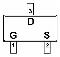
Features: ·N-Channel 20V/0.65A,RDS(ON)=380mΩ@VGS=4.5V 20V/0.55A,RDS(ON)=450mΩ@VGS=2.5V20V/0.45A,RDS(ON)=800mΩ@VGS=1.8V·Super high density cell design for extremely low RDS (ON)·Exceptional on-resistance and maximum DC current capability·SOT-523 (SC-89) package designApplication·D...
SPN1012: Features: ·N-Channel 20V/0.65A,RDS(ON)=380mΩ@VGS=4.5V 20V/0.55A,RDS(ON)=450mΩ@VGS=2.5V20V/0.45A,RDS(ON)=800mΩ@VGS=1.8V·Super high density cell design for extremely low RDS (ON)·Exc...
SeekIC Buyer Protection PLUS - newly updated for 2013!
268 Transactions
All payment methods are secure and covered by SeekIC Buyer Protection PLUS.

| Parameter | Symbol | Typical | Unit | |
| Drain-Source Voltage | VDSS | 20 | V | |
| Gate Source Voltage | VGSS | ±12 | V | |
| Continuous Drain Current(TJ=150 ) | TA=25 | ID | 0.65 | A |
| TA=70 | 0.45 | |||
| Pulsed Drain Current | IDM |
1.0 | A | |
| Continuous Source Current(Diode Conduction) | IS | 0.3 | A | |
| Power Dissipation | TA=25 | PD | 0.27 | W |
| TA=70 | 0.16 | |||
| Operating Junction Temperature |
TJ | -55/150 | ||
| Storage Temperature Range | TSTG | -55/150 | ||
The SPN1012 is the N-Channel enhancement mode power field effect transistors are produced using high cell density , DMOS trench technology. This high density process is especially tailored to minimize on-state resistance and provide superior switching performance. These devices are particularly suited for low voltage applications such as notebook computer power management and other battery powered circuits where high-side switching , low in-line power loss, and resistance to transients are needed.