Features: 128x64/80 + 1 icon line, 4 gray-levels Graphic DisplayProgrammable Multiplex ratio [16Mux - 65Mux/81Mux]Single Supply Operation, 1.8 V - 3.3VLow Current Sleep Mode(<1.0 uA)On-Chip Voltage Generator / External Power SupplySoftware selectable 2X / 3X / 4X / 5X / 6X On-Chip DC-DC Convert...
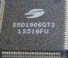
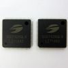
SSD1851: Features: 128x64/80 + 1 icon line, 4 gray-levels Graphic DisplayProgrammable Multiplex ratio [16Mux - 65Mux/81Mux]Single Supply Operation, 1.8 V - 3.3VLow Current Sleep Mode(<1.0 uA)On-Chip Volta...
SeekIC Buyer Protection PLUS - newly updated for 2013!
268 Transactions
All payment methods are secure and covered by SeekIC Buyer Protection PLUS.
Symbol | Parameter | Value | Unit |
VDD | Supply voltage | -0.3 to 4.0 | V |
VCC | VSS-0.3 to VSS+18.0 |
V | |
VCI | Booster Supply Voltage | VDD to 4.0 | V |
Vin | Input Voltage | VSS-0.3 to VDD+0.3 |
V |
I | Current Drain Per Pin Excluding VDD and VSS | 25 | mA |
TA | Operating Temperature | -40 to +80 | oC |
Tstg | Storage Temperature Range | -65 to +150 | oC |
SSD1851 determines whether the input data is interpreted as data or command. Data is directed to this module based upon the input of the D/C pin. If D/C is high, data is written to Graphic Display Data RAM (GDDRAM). If D/C is low, the input of SSD1851 at D0-D7 is interpreted as a Command and it will be decoded and written to the corresponding command register.
Reset is of the same function as Power ON Reset (POR). Once RES receives a negative reset pulse of about 1us, all internal circuitry of SSD1851 will be back to its initial status. Refer to Command Description section for more information.
The parallel interface of SSD1851 consists of 8 bi-directional data pins (D0-D7), R/W( WR ), D/C , E(RD ) and CS . R/W( WR ) input High indicates a read operation from the Graphic Display Data RAM (GDDRAM) or the status register. R/W( WR ) input Low indicates a write operation to Display Data RAM or Internal Command Registers depending on the status of D/C input. The E(RD ) and CS input serves as data latch signal (clock) when they are high and low respectively. Refer to P.35, Figure 1 of parallel timing characteristics for Parallel Interface Timing Diagram of 6800-series microprocessors.
In order to match the operating frequency of display RAM with that of the microprocessor, pipeline processing is internally performed which requires the insertion of a dummy read before the first actual display data read. This is shown in Figure 4 below.