Features: • Single Voltage Read and Write Operations
5.0V-only for the 28SF040
3.0V-only for the 28LF040
2.7V-only for the 28VF040
• Superior Reliability
Endurance: 100,000 Cycles (typical)
Greater than 100 years Data Retention
• Memory Organization: 512K x 8
• Sector Erase Capability: 256 bytes per Sector
• Low Power Consumption
Active Current: 15 mA (typical) for 5.0V and 10 mA (typical) for 3.0/2.7V
Standby Current: 5 A (typical)
• Fast Sector Erase/Byte Program Operation
Byte Program Time: 35 s (typical)
Sector Erase Time: 2 ms (typical)
Complete Memory Rewrite: 20 sec (typical)
• Fast Read Access Time
5.0V-only operation: 120 and 150 ns
3.0V-only operation: 200 and 250 ns
2.7V-only operation: 250 and 300 ns
• Latched Address and Data
• Hardware and Software Data Protection
7-Read-Cycle-Sequence Software Data Protection
• End of Write Detection
Toggle Bit
Data# Polling
• TTL I/O Compatibility
• Packages Available
32-Pin TSOP (8 mm x 20 mm)
32-Pin PLCC
32-Pin PDIPPinout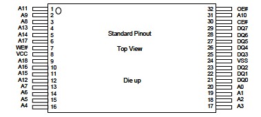 Specifications
Applied conditions greater than those listed under "Absolute Maximum Stress Ratings" may cause permanent
damage to the device. This is a stress rating only and functional operation of the device at these conditions or
conditions greater than those defined in the operational sections of this data sheet is not implied.Exposure to
absolute maximum stress rating conditions may affect device reliability
Temperature Under Bias ........................................................................................................ -55 to +125
Storage Temperature ......................................................................................................... ... -65 to +150
D. C. Voltage on Any Pin to Ground Potential ................................................................... -0.5V to VCC+ 0.5V
Transient Voltage (<20 ns) on Any Pin to Ground Potential ............................................. -1.0V to VCC+ 1.0V
Voltage on A9 Pin to Ground Potential ..................................................................................... -0.5V to 14.0V
Package Power Dissipation Capability (Ta = 25) ...................................................................... ........... 1.0W
Through Hole Soldering Temperature (10 Seconds) ............................................................................... 300
Surface Mount Lead Soldering Temperature (3 Seconds) ..................................................................... . 240
Output Short Circuit Current(1) ........................................................................................................... 100 mA
DescriptionThe SST28VF040 are 512K x 8 bit CMOS sector erase, byte program EEPROMs. The 28SF040/28LF040/28VF040 are manufactured using SST's proprietary, high performance CMOS SuperFlash EEPROM Technology. The split gate cell design and thick oxide tunneling injector attain better reliability and manufacturability compared with alternative approaches. The 28SF040/28LF040/28VF040 erase and program with a single power supply. The 28SF040/ 28LF040/28VF040 conform to JEDEC standard pinouts for byte wide memories and are compatible with existing industry standard EPROM, flash EPROM and EEPROM pinouts.
Featuring high performance programming, the SST28VF040 typically byte program in 35 s. The 28SF040/28LF040/28VF040 typically sector erase in 2 ms. Both program and erase times can be optimized using interface features such as Toggle bit or Data# Polling to indicate the completion of the write cycle. To protect against an inadvertent write, the 28SF040/28LF040/28VF040 have on chip hardware and software data protection schemes. Designed, manufactured, and tested for a wide spectrum of applications,the 28SF040/28LF040/28VF040 are offered with a guaranteed sector endurance of 104 or 103 cycles. Data retention is rated greater than 100 years.
The SST28VF040 are best suited for applications that require reprogrammable nonvolatile mass storage of program, configuration, or data memory. For all system applications, the 28SF040/28LF040/28VF040 significantly improve performance and reliability, while lowering power consumption when compared with floppy diskettes or EPROM approaches.EEPROM technology makes possible convenient and economical updating of codes and control programs online.The 28SF040/28LF040/28VF040 improve flexibility,while lowering the cost of program and configuration storage application.
The functional block diagram shows the functional blocks of the SST28VF040. Figures 1 and 2 show the pin assignments for the 32 pin TSOP, 32 pin PDIP, and 32 pin PLCC packages. Pin description and operation modes are described in Tables 1 through 4.

 SST28VF040 Data Sheet