Features: • Flash Organization: 1M x16 or 2M x8
• Dual-Bank Architecture for Concurrent Read/Write Operation
16 Mbit: 4 Mbit + 12 Mbit
• (P)SRAM Organization:
2 Mbit: 128K x16 or 256K x8
4 Mbit: 256K x16 or 512K x8
8 Mbit: 512K x16 or 1024K x8
• Single 2.7-3.3V Read and Write Operations
• Superior Reliability
Endurance: 100,000 Cycles (typical)
Greater than 100 years Data Retention
• Low Power Consumption:
Active Current: 25 mA (typical)
Standby Current: 20 A (typical)
• Hardware Sector Protection (WP#)
Protects 4 outer most sectors (4 KWord) in the larger bank by holding WP# low and unprotects by holding WP# high
• Hardware Reset Pin (RST#)
Resets the internal state machine to reading data array
• Byte Selection for Flash (CIOF pin)
Selects 8-bit or 16-bit mode
• Sector-Erase Capability
Uniform 2 KWord sectors
• Block-Erase Capability
Uniform 32 KWord blocks
• Read Access Time
Flash: 70 ns
(P)SRAM: 70 ns
• Erase-Suspend / Erase-Resume Capabilities
• Security ID Feature
SST: 128 bits
User: 128 bits
• Latched Address and Data
• Fast Erase and Word-/Byte-Program (typical):
Sector-Erase Time: 18 ms
Block-Erase Time: 18 ms
Chip-Erase Time: 35 ms
Word-Program Time: 7 s
• Automatic Write Timing
Internal VPP Generation
• End-of-Write Detection
Toggle Bit
Data# Polling
Ready/Busy# pin
• CMOS I/O Compatibility
• JEDEC Standard Command Set
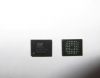
• Packages Available
56-ball LFBGA (8mm x 10mm)
62-ball LFBGA (8mm x 10mm)SpecificationsOperating Temperature . . . . . . . . . . . . . . . . . . . . . ...................... -20°C to +85°C
Storage Temperature . . . . . . . . . . . . . . . . . . . . .. ....................... -65°C to +125°C
D. C. Voltage on Any Pin to Ground Potential . . . . . . . ........... ..-0.5V to VDD 1+0.3V
Transient Voltage (<20 ns) on Any Pin to Ground Potential . . . -1.0V to VDD 1+1.0V
Package Power Dissipation Capability (Ta = 25°C) . . . . . . . . . . . . . . . . . . ... .. 1.0W
Output Short Circuit Current2. . . . . . . . . . . . . . . . . . . . . . . . . . . . . . . . .. . . ... 50 mA
1. VDD = VDDF and VDDS
2. Outputs shorted for no more than one second. No more than one output shorted at a time.DescriptionThe SST34HF1622C ComboMemory devices integrate either a 1M x16 or 2M x8 CMOS flash memory bank with either a 128K x16/256K x8, 256K x16/512 x8, or 512K x16/1024K x8 CMOS SRAM or pseudo SRAM (PSRAM) memory bank in a multi-chip package (MCP). These devices are fabricated using SST's proprietary, high-performance CMOS SuperFlash technology incorporating the split-gate cell design and thick-oxide tunneling injector to attain better reliability and manufacturability compared with alternate approaches. The SST34HF16x2C/D/S devices are ideal for applications such as cellular phones, GPS devices, PDAs, and other portable electronic devices in a low power and small form factor system.
The SST34HF1622C feature dual flash memory bank architecture allowing for concurrent operations between the two flash memory banks and the (P)SRAM. The devices can read data from either bank while an Erase or Program operation is in progress in the opposite bank. The two flashmemory banks are partitioned into 4 Mbit and 12 Mbit with top sector protection options for storing boot code, program code, configuration/parameter data and user data.
The SuperFlash technology provides fixed Erase and Program times, independent of the number of Erase/Program cycles that have occurred. Therefore, the system software or hardware does not have to be modified or de-rated as is necessary with alternative flash technologies, whose Erase and Program times increase with accumulated Erase/Program cycles. The SST34HF16x2C/D/S devices offer a guaranteed endurance of 10,000 cycles. Data retention is rated at greater than 100 years. With high performance Word-Program, the flash memory banks provide a typical Word-Program time of 7 sec. The entire flash memory bank can be erased and programmed word-by-word in typically 4 seconds for the SST34HF16x2C/D/S, when using interface features such as Toggle Bit, Data# Polling, or RY/ BY# to indicate the completion of Program operation. To protect against inadvertent flash write, the SST34HF16x2C/D/S devices contain on-chip hardware and software data protection schemes.
The flash and (P)SRAM operate as two independent memory banks with respective bank enable signals. The memory bank selection is done by two bank enable signals. The (P)SRAM bank enable signals, BES1# and BES2, select the (P)SRAM bank (BES1# and BES2 are NC for SST34HF1602C). The flash memory bank enable signal, BEF#, has to be used with Software Data Protection (SDP) command sequence when controlling the Erase and Program operations in the flash memory bank. The memory banks are superimposed in the same memory address space where they share common address lines, data lines, WE# and OE# which minimize power consumption and area.
Designed, manufactured, and tested for applications requiring low power and small form factor, the SST34HF16x2C/ D/S are offered in both commercial and extended temperatures and a small footprint package to meet board space constraint requirements. See Figures 3 and 4 for pin assignments.

 SST34HF1622C Data Sheet