Features: 16-bit CPU with DSP functions 31.25 ns instruction cycle time at 64MHz max CPU clock Multiply/accumulate unit (MAC) 16 x 16-bit multiplication, 40-bit accumulator Enhanced boolean bit manipulations Single-cycle context switching support On-chip memories 128 Kbyte Flash memory (32-b...
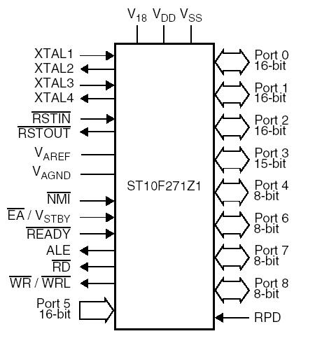
ST10F271Z1: Features: 16-bit CPU with DSP functions 31.25 ns instruction cycle time at 64MHz max CPU clock Multiply/accumulate unit (MAC) 16 x 16-bit multiplication, 40-bit accumulator Enhanced boolean bit ...
SeekIC Buyer Protection PLUS - newly updated for 2013!
268 Transactions
All payment methods are secure and covered by SeekIC Buyer Protection PLUS.
Features: SpecificationsDescription This is the description of ST10 family: This programming manu...

| Symbol | Parameter | Values | Unit |
| VDD | Voltage on VDD pins with respect to ground (VSS) | -0.5 to +6.5 | V |
| VSTBY | Voltage on VSTBY pin with respect to ground (VSS) | -0.5 to +6.5 | V |
| VAREF | Voltage on VAREF pins with respect to ground (VSS) | -0.3 to VDD | V |
| VAGND | Voltage on VAREF pins with respect to ground (VSS) | VSS | V |
| VIO | Voltage on any pin with respect to ground (VSS) | -0.5 to VDD + 0.5 | V |
| IOV | Input current on any pin during overload condition | ± 10 | mA |
| ITOV | Absolute sum of all input currents during overload condition | | 75 | | mA |
| TST | Storage temperature | -65 to +150 | °C |
| ESD | ESD Susceptibility (Human Body Model) | 2000 | V |
Note: Stresses above those listed under "Absolute Maximum Ratings" may cause permanent damage to the device. This is a stress rating only and functional operation of the device at these or any other conditions above those indicated in the operational sections of this specification is not implied. Exposure to absolute maximum rating conditions for extended periods may affect device reliability. During overload conditions (VIN > VDD or VIN < VSS) the voltage on pins with respect to ground (VSS) must not exceed the values defined by the Absolute Maximum Ratings.
During Power-on and Power-off transients (including Standby entering/exiting phases), the relationships between voltages applied to the device and the main VDD shall be always respected. In particular power-on and power-off of VAREF shall be coherent with VDD transient, in order to avoid undesired current injection through the on-chip protection diodes.
The architecture of the ST10F271Z1 combines advantages of both RISC and CISC processors and an advanced peripheral subsystem. The block diagram gives an overview of the different on-chip components and the high bandwidth internal bus structure of the ST10F271Z1.