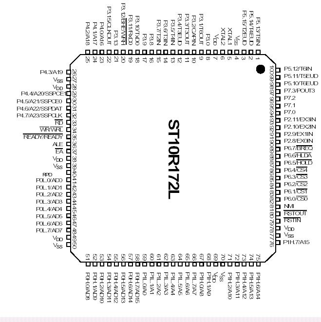
ST10R172L

PinoutSpecifications• Ambient temperature under bias (TA): ..............................................-40°C to +85 °C• Storage temperature (TST):............................................................... 65 to +150 °C• Voltage on VDD pins with respect to ground (VSS):......

product image

ST10R172L Picture
SeekIC No. : 004506167 Detail

ST10R172L: PinoutSpecifications• Ambient temperature under bias (TA): ..............................................-40°C to +85 °C• Storage temperature (TST):.........................................

floor Price/Ceiling Price

Part Number:
ST10R172L
Supply Ability:
5000

Price Break

  • Qty
  • 1~5000
  • Unit Price
  • Negotiable
  • Processing time
  • 15 Days
Total Cost: $ 0.00

SeekIC Buyer Protection PLUS - newly updated for 2013!

  • Escrow Protection.
  • Guaranteed refunds.
  • Secure payments.
  • Learn more >>

Month Sales

268 Transactions

Rating

evaluate  (4.8 stars)

Upload time: 2025/12/23

Payment Methods

All payment methods are secure and covered by SeekIC Buyer Protection PLUS.

Notice: When you place an order, your payment is made to SeekIC and not to your seller. SeekIC only pays the seller after confirming you have received your order. We will also never share your payment details with your seller.
Product Details

Description


Pinout

  Connection Diagram


Specifications

• Ambient temperature under bias (TA): ..............................................-40°C to +85 °C
• Storage temperature (TST):............................................................... 65 to +150 °C
• Voltage on VDD pins with respect to ground (VSS):.............................. 0.5 to +4.0 V
• Voltage on any pin with respect to ground (VSS): ......................... 0.5 to VDD +0.5 V
• Voltage on any 5V tolerant pin with respect to ground (VSS): .................0.5 to 5.5 V
• Voltage on any 5V fail-safe pin with respect to ground (VSS): ................0.5 to 5.5 V
• Input current on any pin during overload condition: ............................ 10 to +10 mA
• Absolute sum of all input currents during overload condition: .........................|100 mA|
• Power dissipation:................................................................................................1.0 W
Note Stresses above those listed under "Absolute Maximum Ratings" may cause permanent damage to the device. This is a stress rating only and functional operation of the device at these or any other conditions above those indicated in the operational sections of this specification is not guaranteed. Exposure to absolute maximum rating conditions for extended periods may affect device reliability. During overload conditions (VIN >VDD or VIN <VSS ) the voltage on pins with respect to ground (VSS ) must not exceed the values defined by the Absolute Maximum Ratings.


Description

ST10R172L architecture combines the advantages of both RISC and CISC processors with an advanced peripheral subsystem. The following block diagram overviews the different onchip components and the internal bus structure.


Customers Who Bought This Item Also Bought

Margin,quality,low-cost products with low minimum orders. Secure your online payments with SeekIC Buyer Protection.
RF and RFID
Power Supplies - Board Mount
Audio Products
Sensors, Transducers
Prototyping Products
DE1
Optical Inspection Equipment
View more