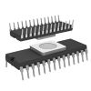
Pinout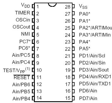
Specifications
|
Symbol |
Parameter |
Value |
Unit |
|
VDD |
Supply Voltage |
-0.3 to 7.0 |
V |
|
VI |
Input Voltage |
VSS - 0.3 to VDD + 0.3(1) |
V |
|
VO |
Output Voltage |
VSS - 0.3 to VDD + 0.3(1) |
V |
|
IVDD |
Total Current into VDD (source) |
80 |
mA |
|
IVSS |
Total Current out of VSS (sink) |
100 |
mA |
|
Tj |
Junction Temperature |
150 |
°C |
|
TSTG |
Storage Temperature |
-60 to 150 |
°C |
DescriptionVDD and VSS. Power is supplied to the MCU via these two pins. VDD is the power connection and VSS is the ground connection.
ST6228C OSCin and OSCout. These pins are internally connected to the on-chip oscillator circuit. A quartz crystal, a ceramic resonator or an external clock signal can be connected between these two pins. The OSCin pin is the input pin, the OSCout pin is the output pin.
ST6228C RESET. The active-low RESET pin is used to restart the microcontroller.
ST6228C TEST/VPP. The TEST must be held at VSS for normal operation. If TEST pin is connected to a +12.5V level during the reset phase, the EPROM/ OTP programming Mode is entered.
ST6228C NMI. The NMI pin provides the capability for asynchronous interruption, by applying an external non maskable interrupt to the MCU. Schmitt trigger characteristics. The user can select as option the availability of an on-chip pull-up at this pin.
ST6228C PA0-PA5. These 6 lines are organised as one I/O port (A). Each line may be configured under software control as inputs with or without internal pullup resistors, input with interrupt generation and pull-up resistor, open-drain or push-pull outputs. PA2/ARTIMout and PA3/ARTIMin can be used respectively as output and input pins for the embedded 8-bit Auto-Reload Timer.
In addition, PA0-PA5 can sink 20mA for direct LED or TRIAC drive.
ST6228C PB4...PB6. These 3 lines are organised as one I/O port (B). Each line may be configured under software control as inputs with or without internal pullup resistors, input with interrupt generation and pull-up resistor, open-drain or push-pull outputs, analog inputs for the A/D converter.
ST6228C PC4-PC7. These 4 lines are organised as one I/O port (C). Each line may be configured under softwarecontrol as input with or without internal pullup resistor, input with interrupt generation and pull-up resistor, open-drain or push-pull output. PC4 and PC5 can also be used as analog input for the A/D converter, while PC6 and PC7 can sink 20mA for direct LED or TRIAC drive.
ST6228C PD1...PD7. These 7 lines are organised as one I/O port (portD). Each line may be configured under software control as input with or without internal pull-up resistor, input with interrupt generation and pull-up resistor, analog input open-drain or pushpull output. In addition, the pins PD5/TXD1 and PD4/RXD1 can be used as UART output (PD5/ TXD1) or UART input (PD4/RXD1). The pins PD3/ Sout, PD2/Sin and PD3/Scl can also be used respectively as data out, data in and clock pins for the on-chip SPI.
ST6228C TIMER. This is the TIMER 1 I/O pin. In input mode, it is connected to the prescaler and acts as external timer clock or as control gate for the internal timer clock. In output mode, the TIMER pin outputs the data bit when a time-out occurs.The user can select as option the availability of an on-chip pullup at this pin.

 ST6228C Data Sheet