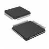
Features: ` Evaluation tool for STEL-1109 digital modulator ASICs
` Burst or continuous BPSK, QPSK, 16QAM modulator at rates up to 10 Msps
` On-board or external clock capability
Up to 165 MHz
` Up to 65 MHz output frequency
` High frequency resolution
24 bits, 10 Hz @ 165 MHz
` Digitally filtered data results in low modulation side lobes
Typically -52 dBc
` High spectral purity
Typically -50 dBc BURST MODE PARAMETERS:
` Default at burst QPSK modulation
Data rate at 2.56 Mbps
` Programmable packet length
1 to 16,381 symbols of data
` Programmable guard time
2 to 16,382 symbols
` Programmable burst quantity
1 to 10 million and auto repeat
` Programmable preamble size
0 to 255 symbols of data
` Master or slave mode
DescriptionThe STEL-1209 is the latest member in Stanford Telecom's line of BPSK/QPSK Burst Modulator board level products. It uses the STEL-1109 ASIC to provide all the convenience of supporting BPSK, QPSK, or 16QAM up-stream modulation with a maximum data rate of 10 Mbps, 20 Mbps, and 40 Mbps; respectively.The STEL-1109 has a Reed-Solomon encoder, a scrambler, a differential encoder, a 10 bit DAC, and many more features needed to build robust communication systems that satisfy today's demanding requirements. For further feature details please refer to the STEL-1109 ASIC data sheet.
Besides the STEL-1109, there is additional logic circuitry implemented in Altera's FPGA to provide burst BPSK, QPSK, and 16QAM modulation modes. Several improvements in these burst modulation modes are included; e.g. external/internal preamble and data sources; variable bursts quantity (includes single to 10 -million and auto repeat); variable packet length, guard time, and preamble size (including zero preamble size). This flexibility allows the STEL-1209 to be customized easily into customers' specific environment. Connectors J3 and J4 are digital test pins provided for easy monitoring of the burst control/signal timing relationships.
With a 0.35 micron ASIC process the STEL-1109 can support a maximum clock frequency of 165 MHz. The frequency of the output modulated carrier is programmable between 5 to 65 MHz; the upper limit is approximately 40% of the master clock. The STEL-1209 has a 102.4 MHz crystal oscillator on-board. Hence, its maximum modulated carrier frequency can be set to 40 MHz. However, an external clock (+10 to +13 dBm) can be selected as the master (through connector J2 and jumper JP4) and carrier frequency of 65 MHz can be achieved easily. An obvious difference between this board and its predecessor (STEL-1208) is the absence of a DAC. A 10 bit DAC is built in the STEL-1109 and observable spur level is -50 dB or better. It has a pair of differential current outputs which swings ±0.96 volt peak-to-peak at 50 ohm termination. Single-ended output of the DAC (using transformer T1 as a double to single-ended converter) can be obtained from J7 (expects 50 or 75 ohm termination impedance from instrumentation). Also included is a choice between two output low pass filters (jumper JP5 and JP6) with cut-off frequency at 42 and 65 MHz. The output of the filter is amplified and is obtainable from J5 (75 ohm source impedance). JP3 routes the DAC output to either J7 or J5.
The STEL-1209 board (running at 102.4 MHz in continuous modulation mode) takes about 430 mA at the 5 volt supply. Power is supplied to the board through JP1. Its pins are clearly labeled on the board (pin 1 = -5 volt, pin 2 = AGND, pin 3 = DGND, pin 4 = VCC (+5 volt)).Reversing the polarity of the supply pins would cause damage to the board. When clock enable line is taken low (grounded), the board consumes 200 mA or less. Current drawn on the -5 volt supply is 10 mA. There are two 5 volt to 3.3 volt converters on the board and the design serves to demonstrate the inter-operability of the STEL-1109 in a 5 volt or 3.3 volt system. The STEL- 1109 ASIC, which is a 3.3V device, consumes 1.8 mA/MHz in continuous mode. Current consumption by the ASIC can be easily measured by connecting pin 2 of JP9 (see package outline) to a 3.3 V power supply that has a current meter.
STEL-1209's operating mode can be modified by writing new values to the STEL-1109 and the burst controller's registers. These registers can be read and written through a Graphical User Interface (GUI) program that comes with the STEL-1209 board. The GUI software allows the user to select different modulation methods, preamble size, interpolation ratio, etc. with the ease of button clicking on a Personal Computer running Microsoft's Windows 95 operating system. A serial cable with 9 pin D-sub connector must be connected between P2 of the STEL -1209 and the PC's COM port for the GUI software to work. At power up or upon reset, the STEL -1209 is automatically loaded with default values to give repeating QPSK burst modulation (50% duty cycle) centered at 10 MHz (master mode). This default mode allows the STEL- 1209 to communicate with the STEL -9244, up-stream burst demodulator. External data must be provided to connector J1 (75 ohm unipolar unbalance) to complete the communication loop. Clock for the external data is provided through connector J6 (75 ohm unipolar unbalance).

 STE1209 Data Sheet


