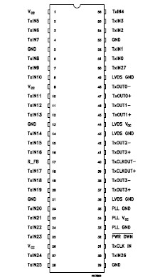
Features: 20 TO 85 MHz SHIFT CLOCK SUPPORTBESTINCLASS SET & HOLD TIMES ON TxINPUTs Tx POWER CONSUMPTION <130 mW (typ)@85MHz GRAYSCALE Tx POWER-DOWN MODE <200W (max) SUPPORTS VGA, SVGA, XGA aND SINGLE/DUAL PIXEL SXGA. NARROW BUS REDUCES CABLE SIZE AND COST UP TO 2.38 Gbps THROUGHPUT UP TO...
STLVDS385: Features: 20 TO 85 MHz SHIFT CLOCK SUPPORTBESTINCLASS SET & HOLD TIMES ON TxINPUTs Tx POWER CONSUMPTION <130 mW (typ)@85MHz GRAYSCALE Tx POWER-DOWN MODE <200W (max) SUPPORTS VGA, SVGA, XGA...
SeekIC Buyer Protection PLUS - newly updated for 2013!
268 Transactions
All payment methods are secure and covered by SeekIC Buyer Protection PLUS.

| Symbol | Parameter | Value | Unit |
| VCC | Supply Voltage | -0.3 to 4 | V |
| VI | CMOS/TTL Input Voltage | -0.5 to (VCC + 0.3) | V |
| VDO | LVDS Driver Output Voltage | -0.3 to (VCC + 0.3) | V |
| IOSD | LVDS Output Short Circuit Duration | Continuous | |
| ESD | HBM | 7 | KV |
| EIAJ | 500 | V | |
| ILATCH | Latch Up Tolerance | ± 300 | mA |
| TJ | Junction Temperature | +150 | °C |
| Tstg | Storage Temperature Range | -65 to +150 | °C |
The STLVDS385 transmitter converts 28 bits of LVCMOS/LVTTL data into four LVDS (Low Voltage Differential Signaling) data streams. A phase-locked transmit clock is transmitted in parallel with the data streams over a fifth LVDS link. Every cycle of the transmit clock 28 bits of input data are sampled and transmitted. At a transmit clock frequency of 85 MHz, 24 bits of RGB data and 3 bits of LCD timing and control data (FPLINE, FPFRAME, DRDY) are transmitted at a rate of 595 Mbps per LVDS data channel.Using a 85 MHz clock, the data throughput is 297.5 Mbytes/sec. The transmitter STLVDS385 can be programmed for Rising edge strobe or Falling edge strobe through a dedicated pin. A Rising edge or Falling edge strobe transmitter will inter operate with a Falling edge strobe Receiver without any translation logic.