Transistor Polarity
: N-Channel
Configuration
: Single
Mounting Style
: Through Hole
Drain-Source Breakdown Voltage
: 650 V
Maximum Operating Temperature
: + 150 C
Packaging
: Tube
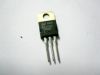
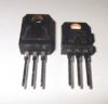
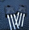
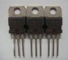
Package / Case
: TO-220
Gate-Source Breakdown Voltage
: +/- 30 V
Continuous Drain Current
: 5 A
Resistance Drain-Source RDS (on)
: 1.8 Ohms
DescriptionThe STP5NK65Z is obtained through an extreme optimization of ST's well estabilished stripbased powerMESH layout. The features of STP5NK65 Z are as follows: (1)typical RDS(on)=1.5 ; (2)extremely high dv/dt capability; (3)100% avlanche tested; (4)gate change minimized; (5)very low intrinsic capacitances; (6)very good manufacturing repeatibility.
The following is about the absolute maximum ratings of STP5NK65Z: (1)drain-source voltage(VGS=0): 650V; (2)drain-gate voltage(VGS=20 k): 650V; (3)gate-source voltage: ±30V; (4)drain current at TC=25: 5 A; (5)drain current at TC=100: 3.1 A; (6)drain current (pulse): 20 A; (7)total dissipation at TC=25: 85 W; (8)derating factor: 0.6 W/; (9)gate source ESD: 2000V; (10)peak diode recovery voltage slope: 4.5 V/ns.
The electrical characteristics of the STP5NK65Z are: (1)drain-source breakdown voltage: 650V min at ID=1mA, VGS=0; (2)zero gate voltage drain source (VGS=0): 1 A max at VDS=max rating and 50 A at VDS=max rating, TC=125; (3)gate-body leakage current (VDS=0): ±10 A at VGS=±20V; (4)gate threshold voltage: 3V min, 3.75V typ and 4.5V max at VGS=VDS, ID=50 A; (5)static drain-source on resistance: 1.5 typ and 1.8 max at VGS=10 V, ID=2.1 A.

 STP5NK65Z Data Sheet