Features: 16/32-bit 96 MHz ARM9E based MCU
ARM966E-S RISC core: Harvard architecture,5-stage pipeline, Tightly-Coupled Memories (SRAM and Flash)
STR91xF implementation of core adds highspeed burst Flash memory interface,instruction prefetch queue, branch cache
Up to 96 MIPS directly from Flash memory
Single-cycle DSP instructions are supported
Binary compatible with 16/32-bit ARM7 code
Dual burst Flash memories, 32-bits wide
256KB/512KB Main Flash, 32KB 2nd Flash
Sequential Burst operation up to 96 MHz
100K min erase cycles, 20 yr min retention
SRAM, 32-bits wide
64K or 96K bytes, optional battery backup
9 programmable DMA channels
One for Ethernet, eight programmablechannels
Clock, reset, and supply management
Two supplies required. Core: 1.8 V +/-10%,I/O: 2.7 to 3.6 V
Internal oscillator operating with external4-25 MHz crystal
Internal PLL up to 96MHz
Real-time clock provides calendar functions,tamper detection, and wake-up functions
Reset Supervisor monitors voltage supplies,watchdog timer, wake-up unit, ext. reset
Brown-out monitor for early warning interrupt
Run, Idle, and Sleep Mode as low as 50 uA
Operating temperature -40 to +85°C
Vectored interrupt controller (VIC)
32 IRQ vectors, 30 intr pins, any can be FIQ
Branch cache minimizes interrupt latency
8-channel, 10-bit A/D converter (ADC)
0 to 3.6V range, 0.7 usec conversion
11 Communication interfaces
10/100 Ethernet MAC with DMA and MII port
USB Full-speed (12 Mbps) slave device
CAN interface (2.0B Active)
3 16550-style UARTs with IrDA protocol
2 Fast I2C™, 400 kHz
2 channels for SPI™, SSI™, or Microwire™
8/16-bit EMI bus on 128 packages
Up to 80 I/O pins (muxed with interfaces)
5 V tolerant, 16 have high sink current(8 mA)
Bit-wise manipulation of pins within a port
16-bit standard timers (TIM)
4 timers each with 2 input capture, 2 output compare, PWM and pulse count modes
3-Phase induction motor controller (IMC)
3 pairs of PWM outputs, adjustable centers
Emergency stop, dead-time gen, tach input
JTAG interface with boundary scan
ARM EmbeddedICE® RT for debugging
In-System Programming (ISP) of Flash
Embedded trace module (ARM ETM9)
Hi-speed instruction tracing, 9-pin interface
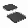
Pinout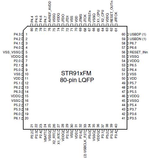 Specifications
|
Symbol |
Parameter |
Min |
Max |
Unit |
|
VDD |
Voltage on VDD pin with respect to ground VSS |
-0.3 |
2.4 |
V |
|
VDDQ |
Voltage on VDDQ pin with respect to ground VSS |
-0.3 |
4.0 |
V |
|
VBATT |
Voltage on VBATT pin with respect to ground VSS |
-0.3 |
4.0 |
V |
|
AVDD |
Voltage on AVDD pin with respect to ground VSS
(128-pinpackage) |
-0.3 |
4.0 |
V |
|
AVREF |
Voltage on AVREF pin with respect to ground VSS
(128-pin package) |
-0.3 |
4.0 |
V |
|
AVREF_AVDD |
Voltage on AVREF_AVDD pin with respect to
Ground VSS (80-pin package) |
-0.3 |
4.0 |
V |
|
VIN |
Voltage on 5V tolerant pins with respect to ground VSS |
-0.3 |
5.5 |
V |
| Voltage on any other pin with respect to ground VSS |
-0.3 |
4.0 |
V |
|
IOV |
Input current on any pin during overload condition |
-10 |
+10 |
mA |
|
ITDV |
Absolute sum of all input currents during overload
condition |
|
|200| |
mA |
|
TST |
Storage Temperature |
-55 |
+150 |
°C |
|
TJ |
Junction Temperature |
|
+125 |
°C |
|
ESD |
ESD Susceptibility (Human Body Model) |
200 |
V |
Note: Stresses exceeding above listed recommended "Absolute Maximum Ratings" may cause permanent damage to the device. This is a stress rating only and functional operation of the device at these or any other conditions above those indicated in the operational sections of this specification is not implied. Exposure to absolute maximum rating conditions for extended periods may affect device reliability. During overload conditions (VIN>VDDQ or VIN<VSSQ) the
voltage on pins with respect to ground (VSSQ) must not exceed the recommended values.

 STR91xF Data Sheet