Transistor Polarity
: N-Channel
Configuration
: Single
Mounting Style
: Through Hole
Maximum Operating Temperature
: + 150 C
Packaging
: Tube
Drain-Source Breakdown Voltage
: 500 V
Continuous Drain Current
: 20 A
Gate-Source Breakdown Voltage
: +/- 30 V
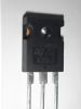
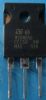
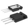
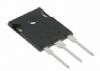
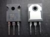
Package / Case
: TO-247
Resistance Drain-Source RDS (on)
: 0.25 Ohms
Application· HIGH CURRENT, HIGH SPEED SWITCHING
· SWITCH MODE POWER SUPPLIES(SMPS)
· DC-AC CONVERTERS FOR WELDING EQUIPMENTAND UNINTERRUPTIBLE POWERSUPPLIES AND MOTOR DRIVESpecifications
| Symbol |
Parameter |
Value |
Unit |
VDS
|
Drain-source Voltage (VGS = 0) |
500 |
V |
| VDGR |
Drain- gate Voltage (RGS = 20 k) |
500 |
V |
| VGS |
Gate-source Voltage |
±30 |
V |
| ID |
Drain Current (continuous) at Tc = 25 |
20 |
A |
| ID |
Drain Current (continuous) at Tc = 100 |
12.7 |
A |
| IDM(•) |
Drain Current (pulsed) |
80 |
A |
| PTOT |
Total Dissipation at Tc = 25 |
250 |
W |
|
Derating Factor |
2 |
W/ |
|
dv/dt(1) |
Peak Diode Recovery voltage slope |
4 |
V/ns |
| Tstg |
Storage Temperature |
-65 to 150 |
|
| Tj |
Max. Operating Junction Temperature |
150 |
|
(•)Pulse width limited by safe operating area
(1)ISD 20A, di/dt 200A/µs, VDD V(BR)DSS, Tj TJMAX.DescriptionUsing the latest high voltage technology,STMicroelectronics STW20NB50 has designed an advanced family of power Mosfets with outstanding performances. The new patent pending strip layout coupled with the Company's proprietary edge termination structure, gives the lowest RDS(on) per area, exceptional avalanche and dv/dt capabilities and unrivalled gate charge and switching characteristics.
Parameters: | Technical/Catalog Information | STW20NB50 |
| Vendor | STMicroelectronics |
| Category | Discrete Semiconductor Products |
| Mounting Type | Through Hole |
| FET Polarity | N-Channel |
| Drain to Source Voltage (Vdss) | 500V |
| Current - Continuous Drain (Id) @ 25° C | 20A |
| Rds On (Max) @ Id, Vgs | 250 mOhm @ 10A, 10V |
| Input Capacitance (Ciss) @ Vds | 4700pF @ 25V |
| Power - Max | 250W |
| Packaging | Tube |
| Gate Charge (Qg) @ Vgs | 110nC @ 10V |
| Package / Case | TO-247 |
| FET Feature | Standard |
| Lead Free Status | Contains Lead |
| RoHS Status | RoHS Non-Compliant |
| Other Names | STW20NB50
STW20NB50
497 2662 5 ND
49726625ND
497-2662-5
|

 STW20NB50 Data Sheet