Features: ` Ideal for customer premise applications` Low standby power consumption:<65 mW per channel` Internal balanced ringing to 65 Vrms` Software programmable parameters:` Ringing frequency, amplitude,cadence, and waveshape` Two-wi...
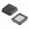
Si3232: Features: ` Ideal for customer premise applications` Low standby power consumption:<65 mW per channel` Internal balanced ringing to 65 Vrms` Software progr...
SeekIC Buyer Protection PLUS - newly updated for 2013!
268 Transactions
All payment methods are secure and covered by SeekIC Buyer Protection PLUS.
| Parameter | Symbol | Test Condition | Value | Unit |
| Supply Voltage, Si3200 and Si3232 | VDD, VDD1VDD4 | 0.5 to 6.0 | V | |
| High Battery Supply Voltage2 | VBATH | Continuous | 0.4 to 104 | V |
| 10 ms | 0.4 to 109 | |||
| Low Battery Supply Voltage, Si32002 | VBAT, VBATL | Continuous | VBATH | V |
| TIP or RING Voltage, Si3200 | VTIP, VRING | Continuous Pulse < 10 s Pulse < 4 s |
104 VBATH 15 VBATH 35 |
V V V |
| TIP, RING Current, Si3200 | ITIP, IRING | ±100 | mA | |
| STIPAC, STIPDC, SRINGAC, SRINGDC Current, Si3232 |
±20 | mA | ||
| Input Current, Digital Input Pins | IIN | Continuous | ±10 | mA |
| Digital Input Voltage | VIND | 0.3 to (VDD + 0.3) | V | |
| Operating Temperature Range | TA | 40 to 100 | °C | |
| Storage Temperature Range | TSTG | 40 to 150 | °C | |
| Si3232 Thermal Resistance, Typical3 (TQFP-64 ePad) |
JA | 25 | °C/W | |
| Si3200 Thermal Resistance, Typical3 (SOIC-16 ePad) |
JA | 55 | °C/W | |
| Continuous Power Dissipation, Si32004 |
PD | TA = 85 °C, SOIC-16 | 1 | W |
| Continuous Power Dissipation, Si3232 |
PD | TA = 85 °C, TQFP-64 | 1.6 | W |
Notes:
1. Permanent device damage may occur if the above Absolute Maximum Ratings are exceeded. Functional operation should be restricted to the conditions as specified in the operational sections of this data sheet. Exposure to absolute
maximum rating conditions for extended periods may affect device reliability.
2. The dv/dt of the voltage applied to the VBAT, VBATH, and VBATL pins must be limited to 10 V/s.
3. The thermal resistance of an exposed pad package is assured when the recommended PCB layout guidelines are followed correctly. The specified performance requires that the exposed pad be soldered to an exposed copper surface of equal size and that multiple vias are added to enable heat transfer between the top-side copper surface and a large internal copper ground plane. Refer to "AN55: Dual ProSLIC™ User Guide" or to the Si3232 evaluation board data sheet for specific layout examples.
4. On-chip thermal limiting circuitry will shut down the circuit at a junction temperature of approximately 150 °C. For
optimal reliability, operation above 140 °C junction temperature should be avoided.
The Si3232 is a low-voltage CMOS SLIC that offers a low-cost, fully softwareprogrammable, dual-channel, analog telephone interface for customer premise (CPE) applications. Internal ringing generation eliminates centralized ringers and ringing relays, and on-chip subscriber loop testing allows remote line card and loop diagnostics with no external test equipment or relays. The Si3232 performs all programmable SLIC functions in compliance with all relevant LSSGR, ITU, and ETSI specifications; all high-voltage functions are performed by the Si3200 linefeed interface IC. The Si3232 operates from a single 3.3 V supply and interfaces to a standard SPI bus digital interface for control. The Si3200 operates from a 3.3 V supply as well as high-voltage battery supplies up to 100 V. The Si3232 is available in a 64-pin thin quad flat package (TQFP), and the Si3200 is available in a thermally-enhanced 16-pin small-outline (SOIC) package.