T2316405A

Features: · Industry-standard x 4 pinouts and timing functions· power supply : T2316405A 2.6V(±0.2V) T2316407A 3.3V(±0.3V)· All device pins are TTL- compatible.· 2048-cycle refresh in 32 ms.· Refresh modes:RAS only,CAS BEFORERAS (CBR) and HIDDEN.· Extended data-out (EDO) PAGE MODE access cycle.Pin...

product image

T2316405A Picture
SeekIC No. : 004511029 Detail

T2316405A: Features: · Industry-standard x 4 pinouts and timing functions· power supply : T2316405A 2.6V(±0.2V) T2316407A 3.3V(±0.3V)· All device pins are TTL- compatible.· 2048-cycle refresh in 32 ms.· Refres...

floor Price/Ceiling Price

Part Number:
T2316405A
Supply Ability:
5000

Price Break

  • Qty
  • 1~5000
  • Unit Price
  • Negotiable
  • Processing time
  • 15 Days
Total Cost: $ 0.00

SeekIC Buyer Protection PLUS - newly updated for 2013!

  • Escrow Protection.
  • Guaranteed refunds.
  • Secure payments.
  • Learn more >>

Month Sales

268 Transactions

Rating

evaluate  (4.8 stars)

Upload time: 2024/5/12

Payment Methods

All payment methods are secure and covered by SeekIC Buyer Protection PLUS.

Notice: When you place an order, your payment is made to SeekIC and not to your seller. SeekIC only pays the seller after confirming you have received your order. We will also never share your payment details with your seller.
Product Details

Description


Features:

· Industry-standard x 4 pinouts and timing functions
· power supply : T2316405A 2.6V(±0.2V) T2316407A 3.3V(±0.3V)
· All device pins are TTL- compatible.
· 2048-cycle refresh in 32 ms.
· Refresh modes: RAS only, CAS BEFORE RAS (CBR) and HIDDEN.
· Extended data-out (EDO) PAGE MODE access cycle.


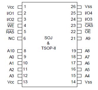
Pinout

  Connection Diagram


Specifications

Parameter
Symbol
Value
Unit
Voltage on Any Pin Relative To Vss
VT
-0.5 to 4.6
V
Supply Voltage Relative To Vss
Vcc
-0.5 to 4.6
V
Short circuit Output Current
Iout
50
mA
Power Dissipation
PT
1
W
Operating Temperature
TOPR
0 to 70
°C
Storage Temperature
Tstg
-55 to 125
°C


Description

The T2316405A and T2316407A is a randomly accessed solid state memory containing 16,777,216 bits organized in a x 4 configuration. T2316405A and T2316407A offer Fast Page mode with Extended Data Output (EDO).

During READ or WRITE cycles, each of the 4 memory bits (1 bit per I/O) is uniquely addressed through the 22 address bits, T2316405A and T2316407A are entered 11 bits (A0-A10) at a time. RAS latches the first 11 bits and CAS latches the latter 11 bits.

A READ or WRITE cycle is selected with the WE input. A logic HIGH on WE dictates READ mode while a logic LOW on WE dictates WRITE mode. During a WRITE cycle, data -in is latched by the falling edge of WE or CAS , whichever occurs last. When WE goes Low prior to CAS going LOW ( EARLY WRITE cycle), the output pins of T2316405A and T2316407A remain open (High-Z) until the next CAS cycle.

A Late Write or Read-Modify-Write occurs. When WE falls after CAS was taken LOW (Late Write cycle). OE must be taken HIGH to disable the data-outputs prior to applying input data.

The four data inputs and four data outputs of T2316405A and T2316407A are routed through four pins using common I/O, and pin direction is controlled by WE and OE .


Customers Who Bought This Item Also Bought

Margin,quality,low-cost products with low minimum orders. Secure your online payments with SeekIC Buyer Protection.
Static Control, ESD, Clean Room Products
Test Equipment
Semiconductor Modules
Memory Cards, Modules
Cables, Wires
Prototyping Products
DE1
View more