TC40107BP

DescriptionTC40107BP DUAL 2-INPUT NAND BUFFER/DRIVER TC40lO7BP is a dual 2-input NAND gate, of which output is of open-drain structure by use of N-channe MOS FET. Being capable of driving a large current, it can be directly connected to a relay, a lamp, a light-emitting diode etc. Wired OR can be ...

product image

TC40107BP Picture
SeekIC No. : 004513616 Detail

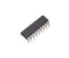
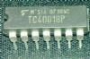
TC40107BP: DescriptionTC40107BP DUAL 2-INPUT NAND BUFFER/DRIVER TC40lO7BP is a dual 2-input NAND gate, of which output is of open-drain structure by use of N-channe MOS FET. Being capable of driving a large cu...

floor Price/Ceiling Price

Part Number:
TC40107BP
Supply Ability:
5000

Price Break

  • Qty
  • 1~5000
  • Unit Price
  • Negotiable
  • Processing time
  • 15 Days
Total Cost: $ 0.00

SeekIC Buyer Protection PLUS - newly updated for 2013!

  • Escrow Protection.
  • Guaranteed refunds.
  • Secure payments.
  • Learn more >>

Month Sales

268 Transactions

Rating

evaluate  (4.8 stars)

Upload time: 2024/4/28

Payment Methods

All payment methods are secure and covered by SeekIC Buyer Protection PLUS.

Notice: When you place an order, your payment is made to SeekIC and not to your seller. SeekIC only pays the seller after confirming you have received your order. We will also never share your payment details with your seller.
Product Details

Description


Description

TC40107BP DUAL 2-INPUT NAND BUFFER/DRIVER TC40lO7BP is a dual 2-input NAND gate, of which output is of open-drain structure by use of N-channe MOS FET. Being capable of driving a large current, it can be directly connected to a relay, a lamp, a light-emitting diode etc. Wired OR can be also made. (IOL=74mA(Typ.) at VDD=10V and VOL=0.5V) The package is a compact DIP 8-pin unit, which is easily mounted. Since its output current is large, if the capacitor of an output line exceeds 500pF, a resistor of 25 or more should be used in series with the capacitor.

The absolute maximum ratings of TC40107BP are (1)DC supply voltage VDD: VSS-0.5~VSS+20V; (2)input voltage VIN: VSS-0.5~VDD+0.5V; (3)output voltage VOUT: VSS-0.5~VDD+0.5V; (4)DC input current IIN: ±10mA; (5)power dissipation PD: 300mW; (6)operating ambient temperature range TA: -40~85°C; (7)storage temperature range Tstg: -65~150°C; (8)lead temp./time Tsol: 260°C`10sec.

The recommended operating conditions of TC40107BP can be summarized as (1)DC supply voltage VDD: 3-18V; (2)input voltage VIN: 0 to VDD V; (3)load capactance CL: 500pF. If you want to know more about this IC, please go to our website for more detail imformation.


Customers Who Bought This Item Also Bought

Margin,quality,low-cost products with low minimum orders. Secure your online payments with SeekIC Buyer Protection.
Programmers, Development Systems
Static Control, ESD, Clean Room Products
LED Products
Audio Products
View more