TC4420

Features: ·Latch-Up Protected ............ Will Withstand >1.5A Reverse Output Current·Logic Input Will Withstand Negative Swing Up to 5V·ESD Protected ..................................................... 4kV·Matched Rise and Fall Times ...................... 25nsec·High Peak Output Current .....

product image

TC4420 Picture
SeekIC No. : 004513711 Detail

TC4420: Features: ·Latch-Up Protected ............ Will Withstand >1.5A Reverse Output Current·Logic Input Will Withstand Negative Swing Up to 5V·ESD Protected ..............................................

floor Price/Ceiling Price

Part Number:
TC4420
Supply Ability:
5000

Price Break

  • Qty
  • 1~5000
  • Unit Price
  • Negotiable
  • Processing time
  • 15 Days
Total Cost: $ 0.00

SeekIC Buyer Protection PLUS - newly updated for 2013!

  • Escrow Protection.
  • Guaranteed refunds.
  • Secure payments.
  • Learn more >>

Month Sales

268 Transactions

Rating

evaluate  (4.8 stars)

Upload time: 2024/4/29

Payment Methods

All payment methods are secure and covered by SeekIC Buyer Protection PLUS.

Notice: When you place an order, your payment is made to SeekIC and not to your seller. SeekIC only pays the seller after confirming you have received your order. We will also never share your payment details with your seller.
Product Details

Description


Features:

·Latch-Up Protected ............ Will Withstand >1.5A Reverse Output Current
·Logic Input Will Withstand Negative Swing Up to 5V
·ESD Protected ..................................................... 4kV
·Matched Rise and Fall Times ...................... 25nsec
·High Peak Output Current ......................... 6A Peak
·Wide Operating Range .......................... 4.5V to 18V
·High Capacitive Load Drive ......................10,000pF
·Short Delay Time ................................. 55nsec Typ.
·Logic High Input, Any Voltage ............. 2.4V to VDD
·Low Supply Current With Logic "1" Input ... 450µA
·Low Output Impedance .................................... 2.5Ω
·Output Voltage Swing to Within 25mV of Ground or VDD


Application

·Switch-Mode Power Supplies
·Motor Controls
·Pulse Transformer Driver
·Class D Switching Amplifiers


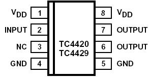
Pinout

  Connection Diagram


Specifications

Parameter NameValuePowerSingle Peak Output Current (mA)6000Output Resistance (RH/RL)(Max. @ 25°C)2.8/2.5Max. Supply Voltage (V)18Input/Output Delay (td1, td2)1 (ns)75/75ConfigurationNon-Inverting DescriptionLow-Side MOSFET Drivers, 2.0A to 9.0A Peak Output CurrentOperating Temp. Range (°C)-40 to 85

Supply Voltage .......................................................................................... +20V
Input Voltage .............................................................................. 5V to > VDD
Input Current (VIN > VDD) ..........................................................................50mA
Power Dissipation, (TA 70°C) PDIP ....................................................730mW
Power Dissipation, (TA 70°C) SOIC ....................................................470mW
Power Dissipation, (TA 70°C) CerDIP ................................................ 800mW
5-Pin TO-220 ..............................................................................................1.6W
Package Power Dissipation, TC 25°C
5-Pin TO-220 (With Heat Sink) .................................................................12.5W
Derating Factors (To Ambient) PDIP ................................................... 8mW/°C
Derating Factors (To Ambient) SOIC ...................................................4mW/°C
Derating Factors (To Ambient) CerDIP .............................................6.4mW/°C
5-Pin TO-220 .................................................................................. 12mW/°C
Thermal Impedances (To Case) 5-Pin TO-220 RJ-C .......................... 10°C/W
Storage Temperature Range .......................................... 65°C to +150°C
Operating Temperature (Chip) .......................................................... +150°C
Operating Temperature Range (Ambient) C Version ................0°C to +70°C
Operating Temperature Range (Ambient) I Version .......... 25°C to +85°C
Operating Temperature Range (Ambient) E Version ......... 40°C to +85°C
Operating Temperature Range (Ambient) M Version ....... 55°C to +125°C
Lead Temperature (Soldering, 10 sec) ................. .............................+300°C


Description

The TC4420/4429 are 6A (peak),single output MOSFET drivers. The TC4429 is an inverting driver (pin-compatible with the TC429), while the TC4420 is a non-inverting driver. These drivers are fabricated in CMOS for lower power, more efficient operation versus bipolar drivers. Both devices have TTL-compatible inputs, which can be driven as high as VDD + 0.3V or as low as 5V without upset or damage to the device. This eliminates the need for external level shifting circuitry and its associated cost and size. The output swing is rail-to-rail ensuring better drive voltage margin, especially during power up/power down sequencing. Propagational delay time is only 55nsec (typ.) and the output rise and fall times are only 25nsec (typ.) into 2500pF across the usable power supply range. Unlike other drivers, the TC4420/4429 are virtually latch-up proof. They replace three or more discrete components saving PCB area, parts and improving overall system reliability.


Customers Who Bought This Item Also Bought

Margin,quality,low-cost products with low minimum orders. Secure your online payments with SeekIC Buyer Protection.
Computers, Office - Components, Accessories
Prototyping Products
DE1
Transformers
Static Control, ESD, Clean Room Products
View more