TD62308BP1G

Features: Two VCC Terminals VCC1, VCC2 (Separated) Package Type BP1G : DIP−16 pin BFG : HSOP−16 pin High Sustaining Voltage Output: VCE (SUS) = 80 V (Min) Output Current (Single Output): IOUT = 1.5 A (Max) Output Clamp Diodes Low Level Active Input GND and SUB Terminal = Heat Sink Inp...

product image

TD62308BP1G Picture
SeekIC No. : 004515895 Detail

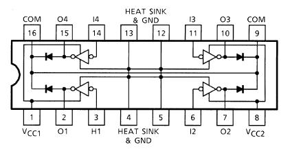
TD62308BP1G: Features: Two VCC Terminals VCC1, VCC2 (Separated) Package Type BP1G : DIP−16 pin BFG : HSOP−16 pin High Sustaining Voltage Output: VCE (SUS) = 80 V (Min) Output Current (Single Output)...

floor Price/Ceiling Price

Part Number:
TD62308BP1G
Supply Ability:
5000

Price Break

  • Qty
  • 1~5000
  • Unit Price
  • Negotiable
  • Processing time
  • 15 Days
Total Cost: $ 0.00

SeekIC Buyer Protection PLUS - newly updated for 2013!

  • Escrow Protection.
  • Guaranteed refunds.
  • Secure payments.
  • Learn more >>

Month Sales

268 Transactions

Rating

evaluate  (4.8 stars)

Upload time: 2024/5/22

Payment Methods

All payment methods are secure and covered by SeekIC Buyer Protection PLUS.

Notice: When you place an order, your payment is made to SeekIC and not to your seller. SeekIC only pays the seller after confirming you have received your order. We will also never share your payment details with your seller.
Product Details

Description


Features:

Two VCC Terminals VCC1, VCC2 (Separated)
Package Type BP1G : DIP−16 pin
                           BFG : HSOP−16 pin
High Sustaining Voltage Output: VCE (SUS) = 80 V (Min)
Output Current (Single Output): IOUT = 1.5 A (Max)
Output Clamp Diodes
Low Level Active Input
GND and SUB Terminal = Heat Sink
Input Compatible with TTL and 5 V CMOS
Standard Supply Voltage


Pinout

  Connection Diagram


Specifications

CHARACTERISTIC SYMBOL RATING UNIT
Supply Voltage VCC 7 V
Output Sustaining Voltage VCE (SUS) −0.5~80 V
Parasitic Transistor Output Voltage VCEF (Note 1) 80 V
Output Current IOUT 1.5 A / ch
Input Current IIN −10 mA
Input Voltage VIN 7 V
Clamp Diode Reverse Voltage VR 80 V
Clamp Diode Forward Current IF 1.5 A
Power Dissipation BP1G PD 1.47 / 2.7 (Note 2) W
BFG 0.9 / 1.4 (Note 3)
Operating Temperature Topr −40~85
Storage Temperature Tstg −55~150
Note 1: Parasitic Transistor (COMMON - GND - OUTPUT) Output Voltage
Note 2: On Glass Epoxy PCB (50 * 50 * 1.6 mm Cu 50%)
Note 3: On Glass Epoxy PCB (60 * 30 * 1.6 mm Cu 30%)


Description

The TD62308BP1G and TD62308BFG are non−inverting transistor array which are comprised of four NPN darlington output stages and PNP input stages.

This device is low level input active driver and are suitable for operation with TTL, 5 V CMOS and 5V Microprocessor which have sink current output drivers.

Applications include relay, hammer, lamp and stepping motor drivers.

The suffix (G) appended to the part number represents a Lead (Pb)-Free product.


Customers Who Bought This Item Also Bought

Margin,quality,low-cost products with low minimum orders. Secure your online payments with SeekIC Buyer Protection.
Potentiometers, Variable Resistors
Computers, Office - Components, Accessories
Industrial Controls, Meters
Line Protection, Backups
Connectors, Interconnects
View more