TDA4661

Features: · Two comb filters, using the switched-capacitor technique, for one line delay time (64 ms)· Adjustment-free application· No crosstalk between SECAM colour carriers (diaphoty)· Handles negative or positive colour-difference input signals· Clamping of AC-coupled input signals (±(R-Y) and ...

product image

TDA4661 Picture
SeekIC No. : 004516365 Detail

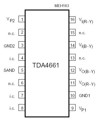
TDA4661: Features: · Two comb filters, using the switched-capacitor technique, for one line delay time (64 ms)· Adjustment-free application· No crosstalk between SECAM colour carriers (diaphoty)· Handles neg...

floor Price/Ceiling Price

Part Number:
TDA4661
Supply Ability:
5000

Price Break

  • Qty
  • 1~5000
  • Unit Price
  • Negotiable
  • Processing time
  • 15 Days
Total Cost: $ 0.00

SeekIC Buyer Protection PLUS - newly updated for 2013!

  • Escrow Protection.
  • Guaranteed refunds.
  • Secure payments.
  • Learn more >>

Month Sales

268 Transactions

Rating

evaluate  (4.8 stars)

Upload time: 2024/5/14

Payment Methods

All payment methods are secure and covered by SeekIC Buyer Protection PLUS.

Notice: When you place an order, your payment is made to SeekIC and not to your seller. SeekIC only pays the seller after confirming you have received your order. We will also never share your payment details with your seller.
Product Details

Description


Features:

· Two comb filters, using the switched-capacitor technique, for one line delay time (64 ms)
· Adjustment-free application
· No crosstalk between SECAM colour carriers (diaphoty)
· Handles negative or positive colour-difference input signals
· Clamping of AC-coupled input signals (±(R-Y) and ±(B-Y))
· VCO without external components
· 3 MHz internal clock signal derived from a 6 MHz CCO, line-locked by the sandcastle pulse (64 ms line)
· Sample-and-hold circuits and low-pass filters to suppress the 3 MHz clock signal
· Addition of delayed and non-delayed output signals
· Output buffer amplifiers
· Comb filtering functions for NTSC colour-difference signals to suppress cross-colour.


Pinout

  Connection Diagram


Specifications

SYMBOL PARAMETER CONDITIONS MIN. MAX. UNIT
VP1 supply voltage (pin 9)   -0.5 +7 V
VP2 supply voltage (pin 1)   -0.5 +7 V
V5 input voltage on pin 5   -0.5 VP + 1.0 V
Vn voltage on pins 11, 12, 14 and 16   -0.5 VP V
Tstg storage temperature   -25 +150
Tamb operating ambient temperature   0 70
VESD electrostatic handling for all pins note 1 - ±500 V
Note
1. Equivalent to discharging a 200 pF capacitor through a 0 series resistor.


Description

The TDA4661 is an integrated baseband delay line circuit with one line delay. It is suitable for decoders with colour-difference signal outputs ±(R-Y) and ±(B-Y).


Customers Who Bought This Item Also Bought

Margin,quality,low-cost products with low minimum orders. Secure your online payments with SeekIC Buyer Protection.
Isolators
Batteries, Chargers, Holders
Undefined Category
Cables, Wires - Management
Audio Products
Circuit Protection
View more