TDA 4340X

Features: • Internal reference voltage source• Adjustment free oscillator with ceramic resonator 456 kHz• Pilot dependent mono/stereo switching with hysteresis• Stereo indicator output• Analogue control of mono/stereo change over (stereo noise control, SNC)• Pil...

product image

TDA 4340X Picture
SeekIC No. : 004516007 Detail

TDA 4340X: Features: • Internal reference voltage source• Adjustment free oscillator with ceramic resonator 456 kHz• Pilot dependent mono/stereo switching with hysteresis• Stereo indica...

floor Price/Ceiling Price

Part Number:
TDA 4340X
Supply Ability:
5000

Price Break

  • Qty
  • 1~5000
  • Unit Price
  • Negotiable
  • Processing time
  • 15 Days
Total Cost: $ 0.00

SeekIC Buyer Protection PLUS - newly updated for 2013!

  • Escrow Protection.
  • Guaranteed refunds.
  • Secure payments.
  • Learn more >>

Month Sales

268 Transactions

Rating

evaluate  (4.8 stars)

Upload time: 2024/4/18

Payment Methods

All payment methods are secure and covered by SeekIC Buyer Protection PLUS.

Notice: When you place an order, your payment is made to SeekIC and not to your seller. SeekIC only pays the seller after confirming you have received your order. We will also never share your payment details with your seller.
Product Details

Description


Features:

• Internal reference voltage source
• Adjustment free oscillator with ceramic resonator 456 kHz
• Pilot dependent mono/stereo switching with hysteresis
• Stereo indicator output
• Analogue control of mono/stereo change over (stereo noise control, SNC)
• Pilot canceller (19 kHz)
• Adjacent channel noise suppression (114 kHz)
• MUTE facility
• Analogue control of deemphasis (high cut control, HCC).
• Stereo inputs for additional signal source at output amplifiers
• Interference noise detector with integrated high-pass filter
• (IF level signal or MPX input)
• MPX input low-pass filter
• Noise blanking at MPX demodulator outputs
• Input and output level adjustable (resistor values)


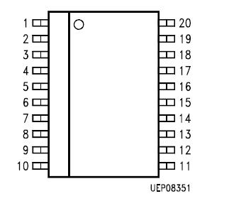
Pinout

  Connection Diagram


Specifications

Parameter
Symbol
Limit Values
Unit
Remarks
min.
max.
PLL loopfilter
V1
0
5
V
 
Oscillator
I2
1
0.1
mA
Reference current
I4
1
0
mA
Supply voltage
V5
0
13.2
V
Noise detector input
V6
0
5
V
Noise gate monoflop
V7
0
V5
V
 
Noise level capacitor
V8
0
V5 1.5
V
 
Output amplifier left
V9
0
6
V
 
AF output left
I10
1
0.3
mA
AF output right
I11
1
0.3
mA
 
Output amplifier right
V12
0
6
V
Deemphasis right
V13
0
5
V
 
Deemphasis left
V14
0
5
V
HCC voltage
V15
0
13.2
V
 
SNC voltage
V16
0
13.2
V
 
Reference level voltage
V17
0
13.2
V
 
Pilot indicator output
I18
0
2
mA
 
Pilot detector output
V19
0
V5 1.5
V
 
MPX input
V20
0
6
V
Junction temperature
Tj
40
150
°C
 
Storage temperature
TS
40
125
°C
Thermal resistance
RthSA
95
K/W
 
ESD voltage, HBM
VESD
4
4
kV
100 pF, 1500 W
Note: Maximum ratings are absolute ratings; exceeding only one of these values may
cause irreversible damage to the integrated circuit.


Customers Who Bought This Item Also Bought

Margin,quality,low-cost products with low minimum orders. Secure your online payments with SeekIC Buyer Protection.
Semiconductor Modules
Cables, Wires - Management
Undefined Category
Optoelectronics
View more