Features: ` High-Density Symmetrically-Blocked Architecture
-Sixteen 64-Kbyte Blocks
` Extended Cycling Capability
-100,000 Block Erase Cycles
-1.6 Million Block Erase Cycles per Chip
` Automated Byte Write and Block Erase
-Command User Interface
-Status Register
` System Performance Enhancements
-RY/BYÝ Status Output
-Erase Suspend Capability
` Deep Power-Down Mode
-0.20 A ICC Typical
` Very High-Performance Read
-85 ns Maximum Access Time
` SRAM-Compatible Write Interface
` Hardware Data Protection Feature
-Erase/Write Lockout during Power Transitions
` Industry Standard Packaging
-40-Lead TSOP, 44-Lead PSOP
` ETOX III Nonvolatile Flash Technology
-12V Byte Write/Block ErasePinout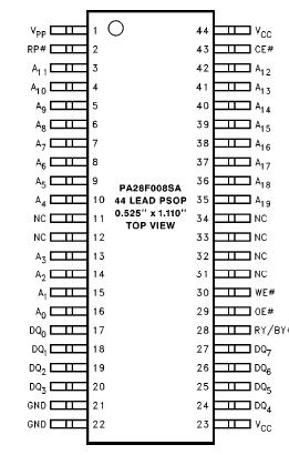 SpecificationsOperating Temperature
During Read ....................................0 to +70(1)
During Block Erase/Byte Write ........0 to +70
Temperature Under Bias .................-10 to +80
Storage Temperature ......................-65 to +125
Voltage on Any Pin
(except VCC and VPP)
with Respect to GND ........................-2.0V to +7.0V(2)
VPP Program Voltage with
Respect to GND during
Block Erase/Byte Write ....................-2.0V to +14.0V(2, 3)
VCC Supply Voltage
with Respect to GND ........................-2.0V to+7.0V(2)
Output Short Circuit Current.............100 mA(4)
NOTES:
1. Operating temperature is for commercial product defined by this specification.
2. Minimum DC voltage is b0.5V on input/output pins. During transitions, this level may undershoot to -2.0V for periods <20 ns. Maximum DC voltage on input/output pins is VCC a 0.5V which, during transitions, may overshoot to VCC +2.0V for periods<20 ns.
3. Maximum DC voltage on VPP may overshoot to +14.0V for periods<20 ns.
4. Output shorted for no more than one second. No more than one output shorted at a time.
5. 5% VCC specifications reference the 28F008SA-85 in its High Speed configuration. 10% VCC specifications reference the 28F008SA-85 in its Standard configuration, and the 28F008SA-120.Description·Intel's 28F008SA 8-Mbit FlashFileTM Memory is the highest density nonvolatile read/write solution for solid- state storage. The 28F008SA's extended cycling, symmetrically blocked architecture, fast access time, write utomation and low power consumption provide a more reliable, lower power, lighter weight and higher performance alternative to traditional rotating disk technology. The 28F008SA brings new capabilities to portable computing.
·Application and operating system software stored in resident flash memory arrays provide instant-on, rapid execute-in-place and protection from obsolescence through in-system software updates.
·Resident software also extends system battery life and increases reliability by reducing disk drive accesses.
·For high density data acquisition applications, the 28F008SA offers a more cost-effective and reliable alternative to SRAM and battery. Traditional high density embedded applications, such as telecommunications, can take advantage of the 28F008SA's nonvolatility, blocking and minimal system code requirements for flexible firmware and modular software designs.
·The 28F008SA is offered in 40-lead TSOP (standard and reverse) and 44-lead PSOP packages. Pin assignments implify board layout when integrating multiple devices in a flash memory array or subsystem. This device uses an integrated Command User Interface and state machine for simplified block erasure and byte write. The 28F008SA memory map consists of 16 separately erasable 64-Kbyte blocks.
·Intel's 28F008SA employs advanced CMOS circuitry for systems requiring low power consumption and noise immunity. Its 85 ns access time provides superior performance when compared with magnetic storage media.
·A deep powerdown mode lowers power consumption to 1 mW typical thru VCC, crucial in portable computing, andheld instrumentation and other low-power applications. The RPÝ power control input also provides absolute data protection during system powerup/down.
·Manufactured on Intel's 0.8 micron ETOX process, the 28F008SA provides the highest levels of quality, reliability and cost-effectiveness.

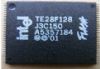
 TE28F008SA-100 Data Sheet