Features: ` Intel SmartVoltage Technology
- 5V or 12V Program/Erase
- 2.7V, 3.3V or 5V Read Operation
- Increased Programming Throughput at 12V VPP
` Very High-Performance Read
- 5V: 60/80/120 ns Max. Access Time, 30/40 ns Max. Output Enable Time
- 3V: 110/150/180 ns Max Access 65/90 ns Max. Output Enable Time
- 2.7V: 120 ns Max Access 65 ns Max. Output Enable Time
` Low Power Consumption
- Max 60 mA Read Current at 5V
- Max 30 mA Read Current at 2.7V3.6V
` x8/x16-Selectable Input/Output Bus
- 28F400 for High Performance 16- or 32-bit CPUs
` x8-Only Input/Output Architecture
- 28F004B for Space-Constrained 8-bit Applications
` Optimized Array Blocking Architecture
- One 16-KB Protected Boot Block
- Two 8-KB Parameter Blocks
- One 96-KB Main Block
- Three 128-KB Main Blocks
- Top or Bottom Boot Locations
` Absolute Hardware-Protection for Boot Block
` Software EEPROM Emulation with Parameter Blocks
` Extended Temperature Operation
- 40 to +85
` Extended Cycling Capability
- 100,000 Block Erase Cycles (Commercial Temperature)
- 10,000 Block Erase Cycles (Extended Temperature)
` Automated Word/Byte Program and Block Erase
- Industry-Standard Command User Interface
- Status Registers
- Erase Suspend Capability
` SRAM-Compatible Write Interface
` Automatic Power Savings Feature
- 1 mA Typical ICC Active Current in Static Operation
` Reset/Deep Power-Down Input
- 0.2 A ICCTypical
- Provides Reset for Boot Operations
` Hardware Data Protection Feature
- Write Lockout during Power Transitions
` Industry-Standard Surface Mount Packaging
- 40-Lead TSOP
- 44-Lead PSOP: JEDEC ROM Compatible
- 56-Lead TSOP
` Footprint Upgradeable from 2-Mbit and
to 8-Mbit Boot Block Flash Memories
` ETOX™ IV Flash TechnologyApplication`The 4-Mbit boot block flash memory family combines high-density, low-power, highperformance, cost-effective flash memories with blocking and hardware protection capabilities. Their flexibility and versatility reduce costs throughout the product life cycle. Flash memory is ideal for Just-In- Time production flow, reducing system inventory and costs, and eliminating component handling during the production phase.
`When your product is in the end-user's hands, and updates or feature enhancements become necessary, flash memory reduces the update costs by allowing user-performed code changes instead of costly product returns or technician calls.
`The 4-Mbit boot block flash memory family provides full-function, blocked flash memories suitable for a wide range of applications. These applications include extended PC BIOS and ROM-able applications storage, digital cellular phone program and data storage, telecommunication boot/firmware, printer firmware/font storage and various other embedded applications where program and data storage are required.
`Reprogrammable systems, such as personal computers, are ideal applications for the 4-Mbit flash memory products. Increasing software sophistication greatens the probability that a code update will be required after the PC is shipped. For example, the emerging of "plug and play" standard in desktop and portable PCs enables autoconfiguration of ISA and PCI add-in cards.
`However, since the "plug and play" specification continues to evolve, a flash BIOS provides a costeffective capability to update existing PCs. In addition, the parameter blocks are ideal for storing the required auto-configuration parameters, allowing you to integrate the BIOS PROM and parameter storage EEPROM into a single component, reducing parts costs while increasing functionality.
`The 4-Mbit flash memory products are also excellent design solutions for digital cellular phone and telecommunication switching applications requiring very low power consumption, highperformance, high-density storage capability, modular software designs, and a small form factor package. The 4-Mbit's blocking scheme allows for easy segmentation of the embedded code with 16 Kbytes of hardware-protected boot code, four main blocks of program code and two parameter blocks of 8 Kbytes each for frequently updated data storage and diagnostic messages (e.g., phone numbers, authorization codes).
`Intel's boot block architecture provides a flexible voltage solution for the different design needs of various applications. The asymmetrically-blocked memory map allows the integration of several memory components into a single flash device. The boot block provides a secure boot PROM; the parameter blocks can emulate EEPROM functionality for parameter store with proper software techniques; and the main blocks provide code and data storage with access times fast enough to execute code in place, decreasing RAM requirements.
Pinout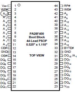 SpecificationsCommercial Operating Temperature
During Read.................................0 to +70
During Block Erase
and Word/Byte Program...............0 to +70
Temperature Bias.....................10 to +80
Extended Operating Temperature
During Read.............................40 to +85
During Block Erase
and Word/Byte Program...........40 to +85
Temperature Under Bias ..........40 to +85
Storage Temperature..............65 to +125
Voltage on Any Pin
(except VCC, VPP, A9 and RP#)
with Respect to GND..............2.0V to +7.0V(2)
Voltage on Pin RP# or Pin A9
with Respect to GND......... 2.0V to +13.5V(2,3)
VPP Program Voltage with Respect
to GND during Block Erase
and Word/Byte Program.... 2.0V to +14.0V(2,3)
VCC Supply Voltage
with Respect to GND................2.0V to +7.0V(2)
Output Short Circuit Current ...............100 mA (4)
1. Operating temperature is for commercial product defined by this specification.
2. Minimum DC voltage is 0.5V on input/output pins. During transitions, this level may undershoot to 2.0V for periods <20 ns. Maximum DC voltage on input/output pins is VCC + 0.5V which, during transitions, may overshoot to VCC + 2.0V for periods <20 ns.
3. Maximum DC voltage on VPP may overshoot to +14.0V for periods <20 ns. Maximum DC voltage on RP# or A9 may overshoot to 13.5V for periods <20 ns.
4. Output shorted for no more than one second. No more than one output shorted at a time.

 TE28F400CET120 Data Sheet