Features: • Supply voltage 2.4 V to 5.5 V, operating idle current (receive mode) < 3.3 mA,shutdown current < 1 A over full temperature range
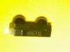
• Surface mount package, top and side view, 9.7 mm x 4.7 mm x 4.0 mm
• Operating temperature - 25 to 85
• Transmitter wavelength typ. 886 nm, supporting IrDA® and remote control
• IrDA® compliant, link distance > 1 m, ± 15, window losses are allowed to still be inside the IrDA® spec.
• Remote control range > 8 m, typ. 22 m
• ESD > 1 kV
• Latchup > 100 mA
• EMI immunity > 550 V/m for GSM frequency and other mobile telephone bands/ (700 MHz to 2000 MHz, no external shield)
• Split power supply, LED can be driven by a separate power supply not loading the regulated supply. U.S. Pat. No. 6,157,476
• Tri-state-receiver output, floating in shut down with a weak pull-up
• Eye safety class 1 (IEC 60825-1, ed. 2001), limited LED on-time, LED current is controlled, no single fault to be considered
• Lead (Pb)-free device
• Qualified for lead (Pb)-free and Sn/Pb processing (MSL4)
• Device in accordance with RoHS 2002/95/EC and WEEE 2002/96EC
Application• Notebook computers, desktop PCs, Palmtop computers (Win CE, Palm PC), PDAs
• Digital still and video cameras
• Printers, fax machines, photocopiers,screen projectors
• Telecommunication products (cellular phones, pagers)
• Internet TV boxes, video conferencing systems
• External infrared adapters (dongles)
• Medical an industrial data collectionSpecifications
|
Parameter |
Test conditions |
Symbol |
Min. |
Typ. |
Max. |
Unit |
Supply voltage range,
transceiver |
0 V < VCC2 < 6 V |
VCC1 |
- 0.5 |
|
+ 6 |
V |
| Supply voltage range, transmitter |
0 V < VCC1 < 6 V |
VCC2 |
- 0.5 |
|
+ 6.5 |
V |
| Input currents |
For all pins, except
IRED anode pin |
|
|
|
10 |
mA |
| Output sinking current |
|
|
|
|
25 |
mA |
| Power dissipation |
See derating curve, figure 5 |
PD |
|
|
500 |
mW |
| Junction temperature |
|
TJ |
|
|
125 |
|
Ambient temperature range
(operating) |
|
Tamb |
- 25 |
|
+ 85 |
|
| Storage temperature range |
|
Tstg |
- 25 |
|
+ 85 |
|
| Soldering temperature |
See recommended solder
profile (see figure 4) |
|
|
|
260 |
|
| Average output current |
|
IIRED(DC) |
|
|
125 |
mA |
| Repetitive pulse output current |
< 90 s, ton < 20 % |
IIRED(RP) |
|
|
600 mA |
|
| IRED anode voltage |
|
VIREDA |
- 0.5 |
|
+ 6.5 |
V |
| Voltage at all inputs and outputs |
Vin > VCC1 is allowed |
VIN |
|
|
5.5 |
V |
DescriptionThe TFDU6103 is a low-power infrared transceiver module compliant to the latest IrDA physical layer standard for fast infrared data communication, supporting IrDA speeds up to 4.0 Mbit/s (FIR), and carrier based remote control modes up to 2 MHz. Integrated within the transceiver module are a PIN photodiode, an infrared emitter (IRED), and a lowpower CMOS control IC to provide a total front-end solution in a single package.
Vishay FIR transceivers are available in different package options, including this BabyFace package (TFDU6103). This wide selection provides flexibility for a variety of applications and space constraints. The transceivers are capable of directly interfacing with a wide variety of I/O devices which perform the modulation/demodulation function, including National Semiconductor's PC87338, PC87108 and PC87109, SMC's FDC37C669, FDC37N769 and CAM35C44, and Hitachi's SH3. TFDU6103 has a tri-state output and is floating in shut-down mode with a weak pull-up.
TFDU6103 datasheet

 TFDU6103 Data Sheet