THS1009

Features: Simultaneous Sampling of Two Single-Ended Signals or One Differential Signals or Combination of BothSignal-to-Noise and Distortion Ratio: 59 dB at fI = 2 MHzDifferential Nonlinearity Error: ±1 LSBIntegral Nonlinearity Error: ±1 LSBAuto-Scan Mode for Two Inputs3-V or 5-V Digital Interface...

product image

THS1009 Picture
SeekIC No. : 004518799 Detail

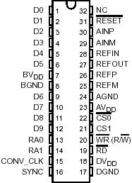
THS1009: Features: Simultaneous Sampling of Two Single-Ended Signals or One Differential Signals or Combination of BothSignal-to-Noise and Distortion Ratio: 59 dB at fI = 2 MHzDifferential Nonlinearity Error...

floor Price/Ceiling Price

Part Number:
THS1009
Supply Ability:
5000

Price Break

  • Qty
  • 1~5000
  • Unit Price
  • Negotiable
  • Processing time
  • 15 Days
Total Cost: $ 0.00

SeekIC Buyer Protection PLUS - newly updated for 2013!

  • Escrow Protection.
  • Guaranteed refunds.
  • Secure payments.
  • Learn more >>

Month Sales

268 Transactions

Rating

evaluate  (4.8 stars)

Upload time: 2024/4/28

Payment Methods

All payment methods are secure and covered by SeekIC Buyer Protection PLUS.

Notice: When you place an order, your payment is made to SeekIC and not to your seller. SeekIC only pays the seller after confirming you have received your order. We will also never share your payment details with your seller.
Product Details

Description


Features:

Simultaneous Sampling of Two Single-Ended Signals or One Differential Signals or Combination of Both
Signal-to-Noise and Distortion Ratio: 59 dB at fI = 2 MHz
Differential Nonlinearity Error: ±1 LSB
Integral Nonlinearity Error: ±1 LSB
Auto-Scan Mode for Two Inputs
3-V or 5-V Digital Interface Compatible
Low Power: 216 mW Max at 5 V
Power Down: 1 mW Max
5-V Analog Single Supply Operation
Internal Voltage References . . . 50 PPM/°C and ±5% Accuracy
Glueless DSP Interface
Parallel µC/DSP Interface


Application

Radar Applications
Communications
Control Applications
High-Speed DSP Front-End
Automotive Applications


Pinout

  Connection Diagram


Specifications


THS10082

Supply voltage range Su ly DGND to DVDD

0.3 V to 6.5 V

BGND to BVDD

0.3 V to 6.5 V

AGND to AVDD

0.3 V to 6.5 V

Analog input voltage range

AGND 0.3 V to AVDD + 1.5 V

Reference input voltage

0.3 V + AGND to AVDD + 0.3 V

Digital input voltage range

0.3 V to BVDD/DVDD + 0.3 V

Operating virtual junction temperature range, TJ

40°C to 150°C

Operating free air temperature range T free-range, TA THS10082C

0°C to 70°C

THS10082I

40°C to 85°C

Storage temperature range, Tstg

65°C to 150°C

Lead temperature 1,6 mm (1/16 inch) from case for 10 seconds

260°C


Description

The THS1009 is a CMOS, low-power, 10-bit, 8 MSPS analog-to-digital converter (ADC). The speed, resolution, bandwidth, and single-supply operation of THS1009 are suited for applications in radar, imaging, high-speed acquisition, and communications. A multistage pipelined architecture with output error correction logic provides for no missing codes over the full operating temperature range. Internal control registers allow forprogramming the ADC into the desired mode. The THS1009 consists of two analog inputs, which are sampled simultaneously. These inputs can be selected individually and configured to single-ended or differential inputs. Internal reference voltages for the ADC (1.5 V and 3.5 V) are provided. An external reference can also be chosen to suit the dc accuracy and temperature drift requirements of the application.

The THS1009C is characterized for operation from 0°C to 70°C, and the THS1009I is characterized for operation from 40°C to 85°C.


Customers Who Bought This Item Also Bought

Margin,quality,low-cost products with low minimum orders. Secure your online payments with SeekIC Buyer Protection.
Optical Inspection Equipment
Crystals and Oscillators
Connectors, Interconnects
Power Supplies - External/Internal (Off-Board)
Memory Cards, Modules
View more