Features: The TLV2262 and TLV2264 are dual and quad low voltage operational amplifiers from Texas Instruments. Both devices exhibit rail-to-rail output performance for increased dynamic range in single or split supply applications. The TLV226x family offers a compromise between the micropower TLV225x and the ac performance of the TLC227x. It has low supply current for battery powered applications, while still having adequate ac performance for applications that demand it.
This family is fully characterized at 3 V and 5 V and is optimized for low-voltage applications. The noise performance has been dramatically improved over previous generations of CMOS amplifiers. Figure 1 depicts the low level of noise voltage for this CMOS amplifier, which has only 200 A (typ) of supply current per amplifier.
The TLV226x, exhibiting high input impedance and low noise, are excellent for small-signal conditioning for highimpedance sources, such as piezoelectric transducers. Because of the micropower dissipation levels combined with 3-V operation, these devices work well in hand-held monitoring and remote-sensing applications. In addition, the rail-to-rail output feature with single or split supplies makes this family a great choice when interfacing with
analog-to-digital converters (ADCs). For precision applications, the TLV226xA family is available and has a maximum input offset voltage of 950 V.
The TLV2262/4 also makes great upgrades to the TLV2332/4 in standard designs. They offer increased output dynamic range, lower noise voltage and lower input offset voltage. This enhanced feature set allows them to
be used in a wider range of applications. For applications that require higher output drive and wider input voltage
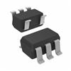
range, see the TLV2432 and TLV2442 devices. If your design requires single amplifiers, please see the TLV2211/21/31 family. These devices are single rail-to-rail operational amplifiers in the SOT-23 package. Their
small size and low power consumption, make them ideal for high density, battery-powered equipment.
ApplicationThe TLV226x is designed to drive larger capacitive loads than most CMOS operational amplifiers. Figure 51
and Figure 52 illustrate its ability to drive loads greater than 400 pF while maintaining good gain and phase
margins (Rnull= 0).
A smaller series resistor (Rnull ) at the output of the device (see Figure 61) improves the gain and phase margins null when driving large capacitive loads. Figure 51 and Figure 52 show the effects of adding series resistances of 10 ?, 20 ?, 50 ?, and 100 ?. The addition of this series resistor has two effects: the first is that it adds a zero to the transfer function and the second is that it reduces the frequency of the pole associated with the output load in the transfer function.
The zero introduced to the transfer function is equal to the series resistance times the load capacitance. To calculate the improvement in phase margin, equation (1) can be used.
The unity-gain bandwidth (UGBW) frequency decreases as the capacitive load increases (see Figure 53). To
use equation 1, UGBW must be approximated from Figure 53. Using equation 1 alone overestimates the improvement in phase margin as illustrated in Figure 59. The overestimation is caused by the decrease in the frequency of the pole associated with the load, providing additional phase shift and reducing the overall improvement in phase margin. The pole associated with the load is reduced by the factor calculated in equation 2.
For the TLV226x, the pole associated with the load is typically 7 MHz with 100-pF load capacitance. This value
varies inversely with CL : at CL = 10 pF, use 70 MHz, at C L = 1000 pF, use 700 kHz, and so on.
Reducing the pole associated with the load introduces phase shift, thereby reducing phase margin. This results
in an error in the increase in phase margin expected by considering the zero alone (equation 1). Equation 3
approximates the reduction in phase margin due to the movement of the pole associated with the load. The
result of this equation can be subtracted from the result of the equation 1 to better approximate the improvement
in phase margin.
Using these equations with Figure 60 and Figure 61 enables the designer to choose the appropriate output
series resistance to optimize the design of circuits driving large capacitive loads.
Pinout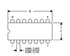 SpecificationsSupply voltage, V (see Note 1) . . . . . . . . . . . . . . . . . . . . . . . . . . . . . . . . . . . . . . . . . . . . . . . . . . . . . . . . . . . . 16 V
DD
Differential input voltage, V (see Note 2) . . . . . . . . . . . . . . . . . . . . . . . . . . . . . . . . . . . . . . . . . . . . . . . . . . . V
ID ± DD
Input voltage range, V (any input, see Note 1) . . . . . . . . . . . . . . . . . . . . . . . . . . . . . . . . . . V -0.3 V to V
I DD- DD+
Input current, I (each input) . . . . . . . . . . . . . . . . . . . . . . . . . . . . . . . . . . . . . . . . . . . . . . . . . . . . . . . . . . . . . . . 5 mA
I ±
Output current, I . . . . . . . . . . . . . . . . . . . . . . . . . . . . . . . . . . . . . . . . . . . . . . . . . . . . . . . . . . . . . . . . . . . . . . . 50 mA
O ±
Total current into V . . . . . . . . . . . . . . . . . . . . . . . . . . . . . . . . . . . . . . . . . . . . . . . . . . . . . . . . . . . . . . . . . . 50 mA
DD+ ±
Total current out of V . . . . . . . . . . . . . . . . . . . . . . . . . . . . . . . . . . . . . . . . . . . . . . . . . . . . . . . . . . . . . . . . 50 mA
DD- ±
Duration of short-circuit current (at or below) 25°C (see Note 3) . . . . . . . . . . . . . . . . . . . . . . . . . . . . . . unlimited
Continuous total power dissipation . . . . . . . . . . . . . . . . . . . . . . . . . . . . . . . . . . . . . See Dissipation Rating Table
Operating free-air temperature range, T : I suffix . . . . . . . . . . . . . . . . . . . . . . . . . . . . . . . . . . . . -40 C to 125 C
A ° °
Q suffix . . . . . . . . . . . . . . . . . . . . . . . . . . . . . . . . . . . -40°C to 125°C
M suffix . . . . . . . . . . . . . . . . . . . . . . . . . . . . . . . . . . -55°C to 125°C
Storage temperature range, T -65. . . . . . . . . . . . . . . . . . . . . . . . . . . . . . . . . . . . . . . . . . . . . . . . . . . C to 150 C
stg ° °
Lead temperature 1,6 mm (1/16 inch) from case for 10 seconds: D, N, P, and PW packages . . . . . . . 260°C
FK, J, JG, U, AND W packages . . 300°C

 TLV226XA Data Sheet