Comparator Type
:
Number of Channels
: 2 Channels
Offset Voltage (Max)
: 5 mV
Mounting Style
: SMD/SMT
Product
: Analog Comparators
Output Type
: Open Collector, Open Drain
Maximum Operating Temperature
: + 85 C
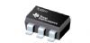
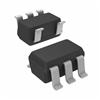
Package / Case
: SOIC-8
Packaging
: Tube
Response Time
: 0.2 us
Maximum Power Dissipation
: 725 mW
Supply Current (Max)
: 0.125 mA
Features: · Wide Range of Supply Voltages 2 V to 8 V
· Fully Characterized at 3 V and 5 V
· Very-Low Supply-Current Drain
120 mA Typ at 3 V
· Output Compatible With TTL, MOS, and
CMOS · Fast Response Time . . . 200 ns Typ for
TTL-Level Input Step
· High Input Impedance . . . 1012 W Typ
· Extremely Low Input Bias Current 5 pA Typ
· Common-Mode Input Voltage Range
Includes Ground
· Built-In ESD ProtectionPinout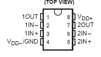 SpecificationsSupply voltage, VDD (see Note 1) . . . . . . . . . . . . . . . . . . . . . . . . . . . . . . . . . . . . . . . . . . . . . . . . . . . . . . .8 V
Differential input voltage, VID (see Note 2) . . . . . . . . . . . . . . . . . . . . . . . . . . . . . . . . . . . . . . . . . . . . . ±8 V
Input voltage range, VI . . . . . . . . . . . . . . . . . . . . . . . . . . . . . . . . . . . . . . . . . . . . . . . . . . . . . . . . 0.3 to 8 V
Output voltage, VO . . . . . . . . . . . . . . . . . . . . . . . . . . . . . . . . . . . . . . . . . . . . . . . . . . . . . . . . . . . . . . . . . 8 V
Input current, II . . . . . . . . . . . . . . . . . . . . . . . . . . . . . . . . . . . . . . . . . . . . . . . . . . . . . . . . . . . . . . . . . .±5 mA
Output current, IO . . . . . . . . . . . . . . . . . . . . . . . . . . . . . . . . . . . . . . . . . . . . . . . . . . . . . . . . . . . . . . . .20 mA
Duration of output short-circuit current to GND (see Note 3) . . . . . . . . . . . . . . . . . . . . . . . . . . . . . unlimited
Continuous total power dissipation . . . . . . . . . . . . . . . . . . . . . . . . . . . . . . . . . See Dissipation Rating Table
Operating free-air temperature range, TA: TLV2352I . . . . . . . . . . . . . . . . . . . . . . . . . . . . . . .40°C to 85°C
TLV2352M . . . . . . . . . . . . . . . . . . . . . . . . . . . . . . . . . . . . . . . . . . . . . . . . . . . . . . . . . . . . . . 55°C to 125°C
Storage temperature range, Tstg . . . . . . . . . . . . . . . . . . . . . . . . . . . . . . . . . . . . . . . . . . . . .65°C to 150°C
Lead temperature 1,6 mm (1/16 inch) from case for 10 seconds: D, P, and PW Packages . . . . . . . . . 260°C
Lead temperature 1,6 mm (1/16 inch) from case for 10 seconds: FK, JG, and U Packages . . . . . . . . 300°C
† Stress beyond those listed under "absolute maximum ratings" may cause permanent damage to the device. These are stress ratings only, and
functional operation of the device at these or any other conditions beyond those indicated under "recommended operating conditions" is not
implied. Exposure to absolute-maximum-rated conditions for extended periods may affect device reliability.
NOTES: 1. All voltage values, except differential voltages, are with respect to network ground.
2. Differential voltages are at IN+ with respect to IN .
3. Short circuits from outputs to VDD can cause excessive heating and eventual device destruction.DescriptionThe TLV2352 consists of two independent, low-power comparators specifically designed for single power-supply applications and operates with power-supply rails as low as 2 V. When powered from a 3-V supply, the typical supply current is only 120 mA.
The TLV2352 is designed using the Texas Instruments LinCMOSE technology and therefore features an extremely high input impedance (typically greater than 1012 W), which allows direct interfacing with high-impedance sources. The outputs are N-channel open-drain configurations that require an external pullup resistor to provide a positive output voltage swing, and they can be connected to achieve positive-logic wired-AND relationships. The TLV2352I is fully characterized at 3 V and 5 V for operation from 40°C to 85°C. The TLV2352M is fully characterized at 3 V and 5 V for operation from 55°C to 125°C.
The TLV2352 has internal electrostatic-discharge (ESD)-protection circuits and has been classified with a 1000-V ESD rating using Human Body Model testing. However, care should be exercised in handling this device as exposure to ESD may result in degradation of the device parametric performance.
Parameters: | Technical/Catalog Information | TLV2352ID |
| Vendor | Texas Instruments |
| Category | Integrated Circuits (ICs) |
| Type | Differential |
| Output Type | CMOS, MOS, Open-Drain, TTL |
| Voltage - Supply | 2 V ~ 8 V |
| Number of Elements | 2 - Dual |
| Package / Case | 8-SOIC (3.9mm Width) |
| Packaging | Tube |
| Drawing Number | 296; 4040047-2; D; 8 |
| Lead Free Status | Lead Free |
| RoHS Status | RoHS Compliant |
| Other Names | TLV2352ID
TLV2352ID
296 10517 5 ND
296105175ND
296-10517-5
|

 TLV2352ID Data Sheet