TPIC6B273

Features: Low rDS(on) ...5 Typical Avalanche Energy ...30 mJ Eight Power DMOS-Transistor Outputs of150-mA Continuous Current 500-mA Typical Current-Limiting Capability Output Clamp Voltage . . . 50 V Low Power ConsumptionPinoutSpecificationsLogic supply voltage, VCC (see Note 1) . . . . . . . ...

product image

TPIC6B273 Picture
SeekIC No. : 004526404 Detail

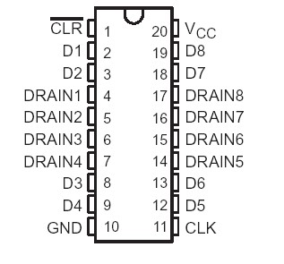
TPIC6B273: Features: Low rDS(on) ...5 Typical Avalanche Energy ...30 mJ Eight Power DMOS-Transistor Outputs of150-mA Continuous Current 500-mA Typical Current-Limiting Capability Output Clamp Voltage . . ....

floor Price/Ceiling Price

Part Number:
TPIC6B273
Supply Ability:
5000

Price Break

  • Qty
  • 1~5000
  • Unit Price
  • Negotiable
  • Processing time
  • 15 Days
Total Cost: $ 0.00

SeekIC Buyer Protection PLUS - newly updated for 2013!

  • Escrow Protection.
  • Guaranteed refunds.
  • Secure payments.
  • Learn more >>

Month Sales

268 Transactions

Rating

evaluate  (4.8 stars)

Upload time: 2024/5/24

Payment Methods

All payment methods are secure and covered by SeekIC Buyer Protection PLUS.

Notice: When you place an order, your payment is made to SeekIC and not to your seller. SeekIC only pays the seller after confirming you have received your order. We will also never share your payment details with your seller.
Product Details

Description


Features:

 Low rDS(on) ...5    Typical
Avalanche Energy ...30 mJ
Eight Power DMOS-Transistor Outputs of150-mA Continuous Current
500-mA Typical Current-Limiting Capability
Output Clamp Voltage . . . 50 V
Low Power Consumption


Pinout

  Connection Diagram


Specifications

Logic supply voltage, VCC (see Note 1) . . . . . . . . . . . . . . . . . . . . . . . . . . . . . . . . . . . . . . . . . 7 V
Logic input voltage range, VI  . . . . . . . . . . . . . . . . . . . . . . . . . . . . . . . . . . . . . . . . . 0.3 V to 7 V
Power DMOS drain-to-source voltage, VDS (see Note 2) . . . . . . . . . . . . . . . . . . . . . . . . . . . 50 V
Continuous source-to-drain diode anode current . . . . . . . . . . . . . . . . . . . . . . . . . . . . . .. .500mA
Pulsed source-to-drain diode anode current (see Note 3) . . . . . . . . . . . . . . . . . . . . . . . . . . ..1 A
Pulsed drain current, each output, all outputs on, ID, TC = 25°C (see Note 3)  . . . . . . . . . 500mA
Continuous drain current, each output, all outputs on, ID, TC = 25°C  . . . . . . . . . . . . . . 150 mA
Peak drain current single output, TC = 25°C (see Note 3)  . . . . . . . . . . . . . . . . . . . . . . . . . 500mA
Single-pulse avalanche energy, EAS (see Figure 4)  . . . . . . . . . . . . . . . . . . . . . . . . . . . . . . 30 mJ
Avalanche current, IAS (see Note 4)  . . . . . . . . . . . . . . . . . . . . . . . . . . . . . . . . . . . . . . . . .500mA
Continuous total dissipation  . . . . . . . . . . . . . . . . . . . . . . . . . . . . . . See Dissipation Rating Table
Operating virtual junction temperature range, TJ . . . . . . . . . . . . . . . . . . . . . . . . 40°C to 150°C
Operating case temperature range, T . . . . . . . . . . . . . . . . . . . . . . . . . . . . . . . .40°C to 125°C
Storage temperature range    . . . . . . . . . . . . . . . . . . . . . . . . . . . . . . . . . . . . .  . . 65°C to 150°C
Lead temperature 1,6 mm (1/16 inch) from case for 10 seconds . . . . . . . . . . . . . . . . . . . . .260°C 


Description

The TPIC6B273 is a monolithic, high-voltage, medium-current, power logic octal D-type latch with DMOS-transistor outputs designed for use in systems that require relatively high load power. The device contains a built-in voltage clamp on the outputs for inductive transient protection. Power driver applications include relays, solenoids, and other medium-current or high-voltage loads.

The TPIC6B273 contains eight positive-edgetriggered D-type flip-flops with a direct clear input. Each flip-flop features an open-drain power DMOS-transistor output.

When clear (CLR) is high, information at the D inputs meeting the setup time requirements is transferred to the DRAIN outputs on the positivegoing edge of the clock (CLK) pulse. Clock triggering occurs at a particular voltage level and is not directly related to the transition time of the positive-going pulse. When the clock input (CLK) is at either the high or low level, the D input signal has no effect at the output. An asynchronous CLR is provided to turn all eight DMOS-transistor outputs off. When data is low for a given output, the DMOS-transistor output is off. When data is high, the DMOS-transistor output has sink-current capability. Outputs of TPIC6B273 are low-side, open-drain DMOS transistors with output ratings of 50 V and 150-mA continuous sink-current capability. Each output of TPIC6B273 provides a 500-mA typical current limit at TC = 25°C. The current limit decreases as the junction temperature increases for additional device protection.

The TPIC6B273 is characterized for operation over the operating case temperature range of 40°C to 125°C. 


Customers Who Bought This Item Also Bought

Margin,quality,low-cost products with low minimum orders. Secure your online payments with SeekIC Buyer Protection.
Crystals and Oscillators
Undefined Category
Sensors, Transducers
Soldering, Desoldering, Rework Products
RF and RFID
View more