TPS1120Y

Features: Low rDS(on) . . . 0.18 at VGS = 10 V3-V CompatibleRequires No External VCCTTL and CMOS Compatible InputsVGS(th) = 1.5 V MaxESD Protection Up to 2 kV per MIL-STD-883C, Method 3015PinoutSpecifications UNIT Drain-to-source voltage, VDS 15 V Gate-to-source voltage, VGS ...

product image

TPS1120Y Picture
SeekIC No. : 004526471 Detail

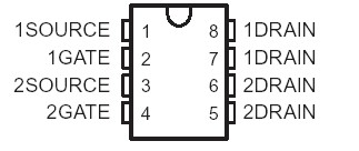
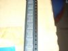
TPS1120Y: Features: Low rDS(on) . . . 0.18 at VGS = 10 V3-V CompatibleRequires No External VCCTTL and CMOS Compatible InputsVGS(th) = 1.5 V MaxESD Protection Up to 2 kV per MIL-STD-883C, Method 3015PinoutSpe...

floor Price/Ceiling Price

Part Number:
TPS1120Y
Supply Ability:
5000

Price Break

  • Qty
  • 1~5000
  • Unit Price
  • Negotiable
  • Processing time
  • 15 Days
Total Cost: $ 0.00

SeekIC Buyer Protection PLUS - newly updated for 2013!

  • Escrow Protection.
  • Guaranteed refunds.
  • Secure payments.
  • Learn more >>

Month Sales

268 Transactions

Rating

evaluate  (4.8 stars)

Upload time: 2024/4/28

Payment Methods

All payment methods are secure and covered by SeekIC Buyer Protection PLUS.

Notice: When you place an order, your payment is made to SeekIC and not to your seller. SeekIC only pays the seller after confirming you have received your order. We will also never share your payment details with your seller.
Product Details

Description


Features:

 Low rDS(on) . . . 0.18 at VGS = 10 V
 3-V Compatible
 Requires No External VCC
 TTL and CMOS Compatible Inputs
 VGS(th) = 1.5 V Max
 ESD Protection Up to 2 kV per MIL-STD-883C, Method 3015


Pinout

  Connection Diagram


Specifications

 
UNIT
Drain-to-source voltage, VDS
15
V
Gate-to-source voltage, VGS
2 or 15
V
Continuous drain current each device (TJ = 150°C) ID
current, C),
VGS = 2.7 V
TA = 25°C
±0.39
A
TA = 125°C
±0.21
VGS = 3 V
TA = 25°C
±0.5
TA = 125°C
±0.25
VGS = 4.5 V
TA = 25°C
±0.74
TA = 125°C
±0.34
VGS = 10 V
TA = 25°C
±1.17
TA = 125°C
±0.53
Pulse drain current, ID
TA = 25°C
±7
A
Continuous source current (diode conduction), IS
TA = 25°C
1
A
Continuous total power dissipation See Dissipation Rating Table
Storage temperature range, Tstg
55 to 150
°C
Operating junction temperature range, TJ
40 to 150
°C
Operating free-air temperature range, TA
40 to 125
°C
Lead temperature 1,6 mm (1/16 inch) from case for 10 seconds
260
°C


Description

The TPS1120Y incorporates two independent p-channel enhancement-mode MOSFETs that have been optimized, by means of the Texas Instruments LinBiCMOSE process, for 3-V or 5-V power distribution in battery-powered systems. With a maximum VGS(th) of 1.5 V and an IDSS of only 0.5 mA, the TPS1120Y is the ideal high-side switch for low-voltage portable battery-management systems, where maximizing battery life is a primary concern. Because portable equipment is potentially subject to electrostatic discharge (ESD), the MOSFETs have built-in circuitry for 2-kV ESD protection. End equipment for the TPS1120Y includes notebook computers, personal digital assistants (PDAs), cellular telephones, bar-code scanners, and PCMCIA cards. For existing designs, the TPS1120D has a pinout common with other p-channel MOSFETs in small-outline integrated circuit SOIC packages.

The TPS1120Y is characterized for an operating junction temperature range, TJ, from 40°C to 150°C.


Customers Who Bought This Item Also Bought

Margin,quality,low-cost products with low minimum orders. Secure your online payments with SeekIC Buyer Protection.
Test Equipment
Optoelectronics
RF and RFID
Cable Assemblies
Power Supplies - External/Internal (Off-Board)
View more