Pinout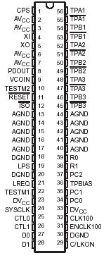 SpecificationsSupply voltage range, VCC . . . . . . . . . . . . . . . . . . . . . . . . . . . . . . . . . . . . . . . . . . . 0.5 V to 6 V
Input voltage range, VI. . . . . . . . . . . . . . . . . . . . . . . . . . . . . . . . . . . .. . . . . . 0.5 V to VCC + 0.5 V
Output voltage range at any output, VO . . . . . . . . . . . . . . . . . . . . . . . . . . . .0.5 V to VCC + 0.5 V
Continuous total power dissipation . . . . . . . . . . . . . . . . . . . . . . . . ..See Dissipation Rating Table
Operating free-air temperature, TA . . . . . . . . . . . . . . . . . . . . . . . . . . . . . . . . . . . . .0°C to 70°C
Storage temperature range . . . . . . . . . . . . . . . . . . . . . . . . . . . . . . . . . . . . . . .65°C to 150°C
Lead temperature 1,6 mm (1/16 inch) from case for 10 seconds . . . . . . . . . . . . . . . . . . . .300°CDescription
The TSB11C01 provides the analog transceiver functions needed to implement a 3-port node in a cable-based IEEE 1394-1995 network. Each cable port incorporates two differential line transceivers. The transceivers include circuitry to monitor the line conditions needed for determining connection status, for initialization and arbitration, and for packet reception and transmission. The TSB11C01 is designed to interface with a link layer controller, such as the TSB12C01A.
The TSB11C01 requires either an external 24.576-MHz crystal or an external 98.304-MHz reference oscillator input. When using the crystal oscillator option, an internal phase-locked loop (PLL) generates the required 98.304-MHz reference signal. Selecting the external oscillator option turns off both the crystal oscillator and the PLL. The 98.304-MHz reference signal is internally divided to provide the 49.152-MHz ±100 ppm clock signals that control transmission of the outbound encoded strobe and data information. The 49.152-MHz clock signal is also supplied to the associated link layer controller for synchronization of the two chips and is used for resynchronization of the received data.
Data bits to be transmitted are received from the link layer controller on two parallel paths and are latched internally in the TSB11C01 in synchronization with the 49.152-MHz system clock. These bits are combined serially, encoded, and transmitted at 98.304 Mbits/s as the outbound data strobe information stream. During transmit, the encoded data information is transmitted differentially on the TPB cable pair(s) and the encoded strobe information is transmitted differentially on the TPA cable pair(s).
During packet reception, the TPA and TPB transmitters of the receiving cable port are disabled and the receivers for that port are enabled. The encoded data information is received on the TPA cable pair, and the encoded strobe information is received on the TPB cable pair. The received data strobe information is decoded to recover the receive clock signal and the serial data bits. The serial data bits are split into two parallel streams, resynchronized to the local system clock and sent to the associated link layer controller. The received data is also transmitted (repeated) out of the other active cable ports
.
Both the TPA and TPB cable interfaces incorporate differential comparators to monitor the line states during initialization and arbitration. The outputs of these comparators are used by the internal logic to determine the arbitration status. In addition, the TPB channel monitors the incoming cable common-mode voltage for the presence of the remotely supplied twisted-pair bias voltage. The presence or absence of this bias voltage is used as an indication of cable connection status.
The TSB11C01 provides a 1.86-V nominal bias voltage for driver load termination. This bias voltage, when seen through a cable by a remote receiver, senses the presence of an active connection. The value of this bias voltage has been chosen to allow interoperability between transceivers operating from either 5-V nominal supplies or 3-V nominal supplies. This bias voltage source should be stabilized by using an external filter capacitor of approximately 1 mF.
The line drivers in the TSB11C01 operate in the high-impedance current mode and are designed to work with external 112-W line matching resistor networks. One network is provided at each end of each twisted-pair cable.
Each network is composed of a pair of series-connected 56-W resistors. The midpoint of the pair of resistors that is directly connected to the twisted-pair A-package terminals is connected to the TPBIAS voltage terminal.
The midpoint of the pair of resistors that is directly connected to the twisted-pair B-package terminals is coupled to ground through a parallel RC network with recommended values of 5 kW and 250 pF. The values of the external resistors are designed to meet the IEEE 1394-1995 specifications when connected in parallel with the internal receiver circuits.
The driver output current, along with other internal operating currents, is set by an external resistor. This resistor is connected between R1 and R0 and has a value of 6.36 kW ±0.5%.
Two terminals set up various test conditions used in manufacturing. Terminals TESTM1 and TESTM2 should be connected to VCC for normal operation.
Four terminals are used as inputs to set four configuration status bits in the self identification packet. These terminals are hardwired high or low as a function of the equipment design. PC[0:2] are three terminals that indicate either the need for power from the cable or the ability to supply power to the cable. The fourth terminal, C/LKON, indicates if a node is a contender for configuration manager. C/LKON can also output a 6.114-MHz ±100 ppm signal, indicating reception of a link-on packet. See Table 427 of the IEEE 1394-1995 standard for additional details.The TSB11C01 supports an optional isolation barrier between itself and its link layer controller. When ISO is tied high, the link interface outputs behave normally; when tied low, an internal differentiating logic is enabled and the outputs become short pulses that can be coupled through a capacitor or transformer.
The TSB11C01 is characterized for operation from 0°C to 70°C.

 TSB11C01 Data Sheet