Features: Controlled Baseline
One Assembly/Test Site, One Fabrication Site
Extended Temperature Performance of
40°C to 110°C
Enhanced Diminishing Manufacturing Sources (DMS) Support
Enhanced Product-Change Notification
Qualification Pedigree†
Fully Supports Provisions of IEEE 1394b-2002 at S100, S100B, S200, S200B, S400, and S400B Signaling Rates (B Signifies 1394b Signaling)
Fully Supports Provisions of IEEE 1394a-2000 and 1394-1995 Standards for High Performance Serial Bus
Fully Interoperable With Firewire™, SB1394™, DishWire™, and i.LINK Implementation of IEEE Std 1394
Provides Three Fully Backward Compatible, (1394a-2000 Fully Compliant) Bilingual 1394b Cable Ports at 400 Megabits per Second (Mbits/s)
Same Three Fully Backward Compatible Ports Are 1394a-2000 Fully Compliant Cable Ports at 100/200/400 Mbits/s
Full 1394a-2000 Support Includes:
Connection Debounce
Arbitrated Short Reset
Multispeed Concatenation
Arbitration Acceleration
Fly-By Concatenation
Port Disable/Suspend/Resume
Extended Resume Signaling for Compatibility With Legacy DV Devices
Power-Down Features to Conserve Energy in Battery Powered Applications
Low-Power Sleep Mode
Automotive Sleep Mode Support
Fully Compliant With Open Host Controller Interface (HCI) Requirements
Cable Power Presence Monitoring
Cable Ports Monitor Line Conditions for Active Connection to Remote Node
Register Bits Give Software Control of Contender Bit, Power Class Bits, Link Active Control Bit, and 1394a-2000 Features
Data Interface to Link-Layer Controller Pin Selectable From 1394a-2000 Mode (2/4/8 Parallel Bits at 49.152 MHz) or 1394b Mode (8 Parallel Bits at 98.304 MHz)
Interface to Link-Layer Controller Supports Low Cost TI Bus-Holder Isolation
Interoperable With Link-Layer Controllers Using 3.3-V Supplies
Interoperable With Other 1394 Physical Layers (PHYs) Using 1.8-V, 3.3-V, and 5-V Supplies
Low Cost 49.152-MHz Crystal Provides Transmit and Receive Data at 100/200/400 Mbits/s, and Link-Layer Controller Clock at 49.152 MHz and 98.304 MHz
Separate Bias (TPBIAS) for Each Port
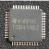
Low Cost, High Performance 80-Pin TQFP (PFP) Thermally Enhanced Package
Software Device Reset (SWR)
Fail-Safe Circuitry Senses Sudden Loss of Power to the Device and Disables the Ports to Ensure That the TSB41BA3 Does Not Load the TPBIAS of Any Connected Device and Blocks Any Leakage From the Port Back to Power Plane
The TSB41BA3 Has a 1394a-2000 Compliant Common-Mode Noise Filter on the Incoming Bias Detect Circuit to Filter Out Cross-Talk Noise
Cable/Transceiver Hardware Speed and Port Mode Are Selectable by Pin States
Supports Connection to CAT5 Cable Transceiver by Allowing Ports to be Forced to Beta-Only 100 Mbits/s only
Supports Connection to S200 Plastic Optical Fiber Transceivers by Allowing Ports to be Forced to1394b Beta-Only 200 Mbits/s and S100 Mbits/s Only
Supports Use of 1394a Connections by Allowing Ports 1 and 2 to Be Forced to 1394a-Only Mode
Optical Signal Detect Input for All Ports in Beta Mode Enables Connection to Optical TransceiversPinout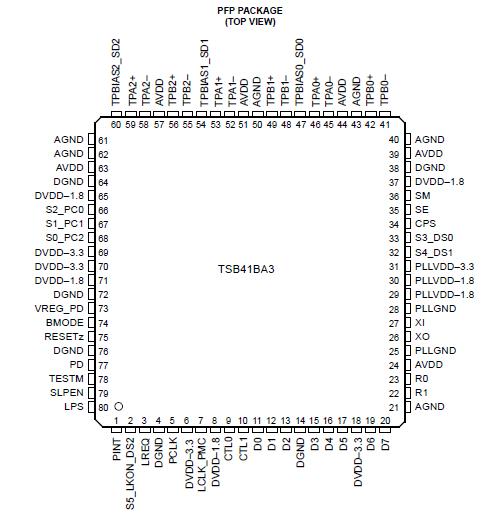 SpecificationsSupply voltage range, VDD (see Note 1) . . . . . . . . . . . . . . . . . . . . . . . . . . . . . . . . . . . . . . . . . . . . 0.3 V to 4 V
Input voltage range, VI (see Note 1) . . . . . . . . . . . . . . . . . . . . . . . . . . . . . . . . . . . . . . . . 0.5 V to VDD + 0.5 V
Output voltage range at any output, VO . . . . . . . . . . . . . . . . . . . . . . . . .. . . . . . . . . . . . . 0.5 V to VDD + 0.5 V
Continuous total power dissipation . . . . . . . . . . . . . . . . . . . . . . . . . . . . . . .. . . . . . See Dissipation Rating Table
Operating free air temperature, TA TSB41BA3T . . . . . . . . . . . . . . . . . . . . .. . . . . . . . . . . . . . . 40°C to110°C
Storage temperature range, Tstg . . . . . . . . . . . . . . . . . . . . . . . . . . . . . . . . . . . . . . . . . . . . . 65°C to 150°C
Lead temperature 1,6 mm (1/16 inch) from case for 10 seconds . . . . . . . . . . . . . . . . . . . . . . . . . . . . . . . 260°C
† Stresses beyond those listed under "absolute maximum ratings" may cause permanent damage to the device. These are stress ratings only, and functional operation of the device at these or any other conditions beyond those indicated under "recommended operating conditions" is not implied. Exposure to absolute-maximum-rated conditions for extended periods may affect device reliability.
NOTE 1: All voltage values, except differential I/O bus voltages, are with respect to network ground.DescriptionThe TSB41BA3-EP provides the digital and analog transceiver functions needed to implement a three-port node in a cable-based IEEE 1394 network. Each cable port incorporates two differential line transceivers. The transceivers include circuitry to monitor the line conditions as needed for determining connection status, for initialization and arbitration, and for packet reception and transmission. The TSB41BA3 is designed to interface with a link-layer controller (LLC), such as the TSB82AA2, TSB12LV21, TSB12LV26, TSB12LV32, TSB42AA4, TSB42AB4, TSB12LV01B, or TSB12LV01C. It may also be connected cable port to cable port to an integrated 1394 Link + PHY layer such as the TSB43AB2.
The TSB41BA3-EP is powered by a single 3.3-V supply. The core voltage supply is supplied by an internal voltage regulator to the PLLVDD-1.8 and DVDD-1.8 terminals. To protect the phase-locked loop (PLL) from noise, the PLLVDD-1.8 terminals must be separately decoupled from the DVDD-1.8 terminals. The PLLVDD-1.8 terminals are decoupled with 1-F and smaller decoupling capacitors, and the DVDD-1.8 terminals are separately decoupled with a 1-F and smaller decoupling capacitors. The separation between DVDD-1.8 and PLLVDD-1.8 must be implemented by separate power supply rails or planes.
The TSB41BA3-EP may be powered by dual supplies, a 3.3-V supply for I/O and a core voltage supply. The core voltage supply is supplied to the PLLVDD-1.8 and DVDD-1.8 terminals to the requirements in the recommended operating conditions section of this data sheet. The PLLVDD-1.8 terminals must be separated from the DVDD-1.8 terminals, the PLLVDD-1.8 terminals are decoupled with 1-F and smaller decoupling capacitors, and the DVDD-1.8 terminals separately decoupled with 1-F and smaller decoupling capacitors. The separation between DVDD-1.8 and PLLVDD-1.8 may be implemented by separate power supply rails, or by a single power supply rail, where the DVDD-1.8 and PLLVDD-1.8 are separated by a filter network to keep noise from the PLLVDD-1.8 supply.
The TSB41BA3-EP requires an external 49.152-MHz crystal to generate a reference clock. The external clock drives an internal phase-locked loop (PLL), which generates the required reference signal. This reference signal provides the clock signals that control transmission of the outbound encoded information. A 49.152-MHz clock signal is supplied by the PHY to the associated LLC for synchronization of the two devices and is used for resynchronization of the received data when operating the PHY-link interface in compliance with the IEEE 1394a-2000 standard. A 98.304-MHz clock signal is supplied by the PHY to the associated LLC for synchronization of the two devices when operating the PHY-link interface in compliance with the IEEE 1394b-2002 standard. The power down (PD) function, when enabled by asserting the PD terminal high, stops operation of the PLL.

 TSB41BA3-EP Data Sheet