Features: • 48 V to 1.5 V V•I Chip Converter
• 90 A (135 A for 1 ms)
• High density 360 A/in3
• Small footprint 84 A/in2
• Low weight 0.5 oz (14 g)
• Pick & Place / SMD
• 125 operation
• 1 s transient response
• >3.5 million hours MTBF
• Typical efficiency 93% at 1.5 V/50 A
• No output filtering required
• BGA or J-Lead packagesApplicationIn applications requiring higher current or redundancy, VTMs can be operated in parallel without adding control circuitry or signal lines. To maximize current sharing accuracy, it is imperative that the source and load impedance on each VTM in a parallel array be equal. If VTMs are being fed by an upstream PRM, the VC nodes of all VTMs must be connectd to the PRM VC.
To achieve matched impedances, dedicated power planes within the PC board should be used for the output and output return paths to the array of paralleled VTMs. This technique is preferable to using traces of varying size and length.
The VTM power train and control architecture allow bi-directional power transfer when the VTM is operating within its specified ranges. Bi-directional power processing improves transient response in the event of an output load dump. The VTM may operate in reverse, returning output power back to the input source. It does so efficiently.
Pinout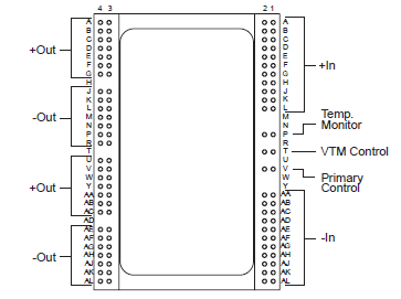 Specifications
|
Parameter |
Values |
Unit |
Notes |
| |
|
|
|
| +In to -In |
-1.0 to 60.0 |
Vdc |
|
| +In to -In |
100 |
Vdc |
For 100 ms |
| PC to -In |
-0.3 to 7.0 |
Vdc |
|
| TM to -In |
-0.3 to 7.0 |
Vdc |
|
| VC to -In |
-0.3 to 19.0 |
Vdc |
|
| +Out to -Out |
-0.1 to 4.0 |
Vdc |
|
| Isolation voltage |
2.250 |
Vdc |
Input to Ouput |
| Operating junction temperature |
-40 to 125
|
|
See Note |
| Output current |
90 |
A |
Continuous |
| Peak output current |
135 |
A |
For 1 ms |
| Case temperature during reflow |
208
|
|
|
| Storage temperature |
-40 to 150
|
|
|
| Output power |
145 |
W |
Continuous |
| Peak output power |
217 |
W |
For 1 ms |
Note: The referenced junction is defined as the semiconductor having the highest temperature. This temperature
is monitored by the temperature monitor (TM) signal and by a shutdown comparator.
DescriptionThe V048K015T090 V•I Chip Voltage Transformation Module (VTM) breaks records for speed, density and efficiency to meet the demands of advanced DSP, FPGA, ASIC, processor cores and microprocessor applications at the point of load (POL) while providing isolation from input to output. It achieves a response time of less than 1 s and delivers up to 90 A in a volume of less than 0.25 in3 while providing low output voltages with unprecedented efficiency. It may be paralleled to deliver hundreds of amps at an output voltage settable from 0.8 to 1.7 Vdc.
The VTM V048K015T090's nominal output voltage is 1.5 Vdc from a 48 Vdc input factorized bus, Vf, and is controllable from 0.8 to 1.7 Vdc at no load, and from 0.8 to 1.6 Vdc at full load, over a Vf input range of 26 to 55 Vdc. It can be operated either open- or closed-loop depending on the output regulation needs of the application. Operating open-loop, the output voltage tracks its Vf input voltage with a transformation ratio, K = 1/32, and an output resistance, ROUT = 1.0 milliohm, to enable applications requiring a programmable low output voltage at high current and high efficiency. Closing the loop back to an input Pre-Regulation Module (PRM) or DC-DC converter can compensate for ROUT.
The V048K015T090 achieves break-through current density of 360 A/in3 in a V•I Chip package compatible with standard pick-and-place and surface mount assembly processes. The V•I Chip BGA package supports in-board mounting with a low profile of 0.16" (4 mm) over the board. A J-lead package option supports on-board surface mounting with a profile of only 0.25" (6 mm) over the board. The V048K015T090's fast dynamic response and low noise eliminate the need for bulk capacitance at the load, substantially increasing the POL density while improving reliability and decreasing cos

 V048K015T090 Data Sheet