V54C365804VC

Features: 4 banks x 2Mbit x 8 organization High speed data transfer rates up to 143 MHz Full Synchronous Dynamic RAM, with all signals referenced to clock rising edge Single PulsedRAS Interface Data Mask for Read/Write Control Four Banks controlled by BA0 & BA1 ProgrammableCAS Latency: 2, 3 P...

product image

V54C365804VC Picture
SeekIC No. : 004539966 Detail

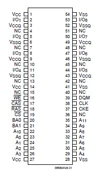
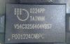
V54C365804VC: Features: 4 banks x 2Mbit x 8 organization High speed data transfer rates up to 143 MHz Full Synchronous Dynamic RAM, with all signals referenced to clock rising edge Single PulsedRAS Interface Dat...

floor Price/Ceiling Price

Part Number:
V54C365804VC
Supply Ability:
5000

Price Break

  • Qty
  • 1~5000
  • Unit Price
  • Negotiable
  • Processing time
  • 15 Days
Total Cost: $ 0.00

SeekIC Buyer Protection PLUS - newly updated for 2013!

  • Escrow Protection.
  • Guaranteed refunds.
  • Secure payments.
  • Learn more >>

Month Sales

268 Transactions

Rating

evaluate  (4.8 stars)

Upload time: 2024/4/29

Payment Methods

All payment methods are secure and covered by SeekIC Buyer Protection PLUS.

Notice: When you place an order, your payment is made to SeekIC and not to your seller. SeekIC only pays the seller after confirming you have received your order. We will also never share your payment details with your seller.
Product Details

Description


Features:

  4 banks x 2Mbit x 8 organization 
  High speed data transfer rates up to 143 MHz 
  Full Synchronous Dynamic RAM, with all signals referenced to clock rising edge 
  Single Pulsed RAS Interface 
  Data Mask for Read/Write Control 
 Four Banks controlled by BA0 & BA1 
  Programmable CAS Latency: 2, 3 
  Programmable Wrap Sequence: Sequential or Interleave 
  Programmable Burst Length:
    1, 2, 4, 8 and full page for Sequential Type
    1, 2, 4, 8 for Interleave Type 
 Multiple Burst Read with Single Write Operation 
  Automatic and Controlled Precharge Command
  Random Column Address every CLK (1-N Rule) 
 Suspend Mode and Power Down Mode 
 Auto Refresh and Self Refresh 
 Refresh Interval: 4096 cycles/64 ms 
 Available in 54 Pin 400 mil TSOP-II
  LVTTL Interface 
  Single +3.3 V±0.3 V Power Supply


Pinout

  Connection Diagram


Specifications

Operating temperature range ..........................................0 to 70 °C
Storage temperature range ....................................... -55 to 150 °C
Input/output voltage ......................................... -0.3 to (VCC+0.3) V
Power supply voltage ................................................... -0.3 to 4.6 V
Power dissipation ....................................................................... 1 W
Data out current (short circuit) ............................................... 50 mA


Description

The V54C365804VC is a four bank Synchronous DRAM organized as 4 banks x 2Mbit x 8. The V54C365804VC achieves high speed data transfer rates up to 143 MHz by employing a chip architecture that prefetches multiple bits and then synchronizes the output data to a system clock

All of the control, address, data input and output circuits are synchronized with the positive edge of an externally supplied clock.

Operating the four memory banks in an interleaved fashion allows random access operation to occur at higher rate than is possible with standard DRAMs. A sequential and gapless data rate of up to 143 MHz is possible depending on burst length, CAS latency and speed grade of the V54C365804VC.


Customers Who Bought This Item Also Bought

Margin,quality,low-cost products with low minimum orders. Secure your online payments with SeekIC Buyer Protection.
Static Control, ESD, Clean Room Products
Cables, Wires - Management
Optical Inspection Equipment
Audio Products
Inductors, Coils, Chokes
Connectors, Interconnects
View more