V58C365164S

Features: 4 banks x 1Mbit x 16 organization High speed data transfer rates with system frequency up to 275 MHz Data Mask for Write Control (DM) Four Banks controlled by BA0 & BA1 Programmable CAS Latency: 2, 2.5, 3 Programmable Wrap Sequence: Sequential or Interleave Programmable Burst Length...

product image

V58C365164S Picture
SeekIC No. : 004540079 Detail

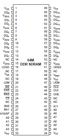
V58C365164S: Features: 4 banks x 1Mbit x 16 organization High speed data transfer rates with system frequency up to 275 MHz Data Mask for Write Control (DM) Four Banks controlled by BA0 & BA1 Programmable C...

floor Price/Ceiling Price

Part Number:
V58C365164S
Supply Ability:
5000

Price Break

  • Qty
  • 1~5000
  • Unit Price
  • Negotiable
  • Processing time
  • 15 Days
Total Cost: $ 0.00

SeekIC Buyer Protection PLUS - newly updated for 2013!

  • Escrow Protection.
  • Guaranteed refunds.
  • Secure payments.
  • Learn more >>

Month Sales

268 Transactions

Rating

evaluate  (4.8 stars)

Upload time: 2024/3/27

Payment Methods

All payment methods are secure and covered by SeekIC Buyer Protection PLUS.

Notice: When you place an order, your payment is made to SeekIC and not to your seller. SeekIC only pays the seller after confirming you have received your order. We will also never share your payment details with your seller.
Product Details

Description


Features:

4 banks x 1Mbit x 16 organization
High speed data transfer rates with system frequency up to 275 MHz
Data Mask for Write Control (DM)
Four Banks controlled by BA0 & BA1
Programmable CAS Latency: 2, 2.5, 3
Programmable Wrap Sequence: Sequential or Interleave
Programmable Burst Length:
   2, 4, 8 for Sequential Type
   2, 4, 8 for Interleave Type
Automatic and Controlled Precharge Command
Suspend Mode and Power Down Mode
Auto Refresh and Self Refresh
Refresh Interval: 4096 cycles/64 ms
Available in 66-pin 400 mil TSOP-II
SSTL-2 Compatible I/Os
Double Data Rate (DDR)
Bidirectional Data Strobe (DQs) for input and output data, active on both edges
On-Chip DLL aligns DQ and DQs transitions with CLK transitions
Differential clock inputs CLK and CLK
Power supply 3.3V ± 0.3V
VDDQ (I/O) power supply 2.5 + 0.2V


Pinout

  Connection Diagram


Specifications

Operating temperature range.......................................0 to 70 °C
Storage temperature range ....................................-55 to 150 °C
Input/output voltage...................................... -0.3 to (VCC+0.3) V
Power supply voltage ............................................... -0.3 to 4.6 V
Power dissipation .................................................................2.0 W
Data out current (short circuit).............................................50 mA


Description

The V58C365164S is a four bank DDR DRAM organized as 4 banks x 1Mbit x 16. The V58C365164S achieves high speed data transfer rates by employing a chip architecture that prefetches multiple bits and then synchronizes the output data to a system clock

All of the control, address, circuits are synchronized with the positive edge of an externally supplied clock. I/O transactions are possible on both edges of DQS.

Operating the four memory banks in an interleaved fashion allows random access operation to occur at a higher rate than is possible with standard DRAMs. A sequential and gapless data rate is possible depending on burst length, CAS latency and speed grade of the device.


Customers Who Bought This Item Also Bought

Margin,quality,low-cost products with low minimum orders. Secure your online payments with SeekIC Buyer Protection.
Integrated Circuits (ICs)
Cable Assemblies
Batteries, Chargers, Holders
Semiconductor Modules
LED Products
Memory Cards, Modules
View more