VS3125

Features: • Enhanced N-FET with no dc path to VCC or GND in normal operating signal voltage range.• Low impedance bidirectional data flow• Pin-compatible with QS3125 & PI5C3125 switches• Zero added ground bounce or signal noise• TTL-compatible control signals...

product image

VS3125 Picture
SeekIC No. : 004543218 Detail

VS3125: Features: • Enhanced N-FET with no dc path to VCC or GND in normal operating signal voltage range.• Low impedance bidirectional data flow• Pin-compatible with QS3125 & PI5C3...

floor Price/Ceiling Price

Part Number:
VS3125
Supply Ability:
5000

Price Break

  • Qty
  • 1~5000
  • Unit Price
  • Negotiable
  • Processing time
  • 15 Days
Total Cost: $ 0.00

SeekIC Buyer Protection PLUS - newly updated for 2013!

  • Escrow Protection.
  • Guaranteed refunds.
  • Secure payments.
  • Learn more >>

Month Sales

268 Transactions

Rating

evaluate  (4.8 stars)

Upload time: 2024/4/29

Payment Methods

All payment methods are secure and covered by SeekIC Buyer Protection PLUS.

Notice: When you place an order, your payment is made to SeekIC and not to your seller. SeekIC only pays the seller after confirming you have received your order. We will also never share your payment details with your seller.
Product Details

Description


Features:

• Enhanced N-FET with no dc path to VCC or GND in normal operating signal voltage range.
• Low impedance bidirectional data flow
• Pin-compatible with QS3125 & PI5C3125 switches
• Zero added ground bounce or signal noise
• TTL-compatible control signals
• Near-zero propagation delay
• Undershoot clamp diodes on all switch and control pins
• ESD rating >2000V (Human Body Model) or >200V (Machine Model)
• Latch-up current >100mA
• Available in 150-mil wide QSOP package


Application

• 5v to 3.3V translation in mixed supply environment
• Hot Swap interface
• Video, audio switching
• Clock gating
• Logic replacement


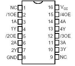
Pinout

  Connection Diagram


Specifications

Supply Voltage to Ground...........-0.5V to +7.0V
DC Switch Voltage VS..............-0.5V to +7.0V
DC Input Voltage VIN..............-0.5V to +7.0V
AC Input Voltage (Pulse Width < 20ns).........-3.0V
DC Output Sink Current per Switch Pin........120 mA
Maximum Power Dissipation.............0.5 Watts
Storage Temperature.............-65 to +150


Description

The VS3125 contains a set of four high-speed, low-resistance bus switches. Each bus switch is individually controlled by TTL-compatible, active-low control input (/xOE). The low ON resistance of VS3125 allows inputs to be connected to outputs without adding propagation delay and without generating additional signal noise.

The VS3125 is function and pinout compatible with QS3125. It enables 5V to 3.3V level translation when used with an external diode in the power supply line. In addition, the high off-isolation between switch terminals in the 'disable' mode, and the near-zero propagation delay in the 'on' state make the VS3V125 an ideal interface element for hot-swapping applications.


Customers Who Bought This Item Also Bought

Margin,quality,low-cost products with low minimum orders. Secure your online payments with SeekIC Buyer Protection.
Optoelectronics
Prototyping Products
DE1
Integrated Circuits (ICs)
Discrete Semiconductor Products
LED Products
RF and RFID
View more