W3E32M64S

Features: · DDR SDRAM rate = 200, 250, 266· Package: • 208 Plastic Ball Grid Array (PBGA), 13 x 22mm· 2.5V ±0.2V core power supply· 2.5V I/O (SSTL_2 compatible)· Differential clock in puts (CK and CK)· Commands entered on each positive CK edge· Internal pipelined double-data-rate (DDR) ar ch...

product image

W3E32M64S Picture
SeekIC No. : 004544675 Detail

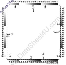
W3E32M64S: Features: · DDR SDRAM rate = 200, 250, 266· Package: • 208 Plastic Ball Grid Array (PBGA), 13 x 22mm· 2.5V ±0.2V core power supply· 2.5V I/O (SSTL_2 compatible)· Differential clock in puts (CK...

floor Price/Ceiling Price

Part Number:
W3E32M64S
Supply Ability:
5000

Price Break

  • Qty
  • 1~5000
  • Unit Price
  • Negotiable
  • Processing time
  • 15 Days
Total Cost: $ 0.00

SeekIC Buyer Protection PLUS - newly updated for 2013!

  • Escrow Protection.
  • Guaranteed refunds.
  • Secure payments.
  • Learn more >>

Month Sales

268 Transactions

Rating

evaluate  (4.8 stars)

Upload time: 2024/3/27

Payment Methods

All payment methods are secure and covered by SeekIC Buyer Protection PLUS.

Notice: When you place an order, your payment is made to SeekIC and not to your seller. SeekIC only pays the seller after confirming you have received your order. We will also never share your payment details with your seller.
Product Details

Description


Features:

· DDR SDRAM rate = 200, 250, 266
· Package: • 208 Plastic Ball Grid Array (PBGA), 13 x 22mm
· 2.5V ±0.2V core power supply
· 2.5V I/O (SSTL_2 compatible)
· Differential clock in puts (CK and CK)
· Commands entered on each positive CK edge
· Internal pipelined double-data-rate (DDR) ar chi tec ture; two data accesses per clock cy cle
· Programmable Burst length: 2,4 or 8
· Bidirectional data strobe (DQS) transmitted/ re ceived with data, i.e., source-syn chro nous data capture (one per byte)
· DQS edge-aligned with data for READs; center-aligned with data for WRITEs
· DLL to align DQ and DQS transitions with CLK
· Four internal banks for concurrent operation
· Data mask (DM) pins for masking write data (one per byte)
· Programmable IOL/IOH option
· Auto precharge option
· Auto Refresh and Self Refresh Modes
· Commercial, Industrial and Military TemperatureRang es
· Organized as 32M x 64
· Weight: W3E32M64S-XSBX - 2 grams typical


Pinout

  Connection Diagram


Specifications

Parameter   Unit
Voltage on VCC, VCCQ Supply relative to Vss -1 to 3.6 V
Voltage on I/O pins relative to Vss -1 to 3.6 V
Operating Temperature TA (Mil) -55 to +125 °C
Operating Temperature TA (Ind) -40 to +85 °C
Storage Temperature, Plastic -55 to +150 v

NOTE:Stress greater than those listed under "Absolute Maximum Ratings" may cause per ma nent damage to the device. This is a stress rating only and func tion al op er a tion of the device at these or any other conditions greater than those in di cat ed in the operational sections of this specifi cation is not implied. Exposure to ab so lute maximum rating con di tions for extended periods may affect reliability.


Description

The 256MByte (2Gb) DDR SDRAM is a high-speed CMOS, dy nam ic ran dom-access, memory using 4 chips containing 536,870,912 bits. Each chip is internally configured as a quad-bank DRAM.

The 256MB DDR SDRAM uses a double data rate ar chi tec ture to achieve high-speed operation. The double data rate ar chi tec ture is essentially a 2n-prefetch architecture with an in ter face designed to transfer two data words per clock cycle at the I/O pins. A single read or write access for the 256MB DDR SDRAM effectively consists of a single 2n-bit wide, one-clock-cycle data tansfer at the internal DRAM core and two cor re spond ing n-bit wide, one-half-clock-cycle data transfers at the I/O pins.

A bi-directional data strobe (DQS) is transmitted externally, along with data, for use in data capture at the receiver.strobe transmitted by the DDR SDRAM during READs and by the memory contoller during WRITEs. DQS is edge-aligned with data for READs and centeraligned with data for WRITEs. Each chip has two data strobes, one for the lower byte and one for the upper byte.

The 256MB DDR SDRAM operates from a differential lock (CK and CK); the crossing of CK going HIGH and CK going LOW will be referred to as the positive edge of CK. Com mands (ad dress and control signals) are registered at every positive edge of CK. Input data is registered on both edg es of DQS, and out put data.


Customers Who Bought This Item Also Bought

Margin,quality,low-cost products with low minimum orders. Secure your online payments with SeekIC Buyer Protection.
Inductors, Coils, Chokes
Potentiometers, Variable Resistors
Power Supplies - Board Mount
Memory Cards, Modules
Prototyping Products
DE1
Cable Assemblies
View more