W6691

Features: • Full Duplex 2B+D S/T interface transceiver compliant with ITU I.430 Recommendation• One D channel HDLC controller− Maskable address recognition− Transparent (HDLC) mode− FIFO buffer (2 * 64)• Two B channel HDLC controller− Maskable address reco...

product image

W6691 Picture
SeekIC No. : 004544903 Detail

W6691: Features: • Full Duplex 2B+D S/T interface transceiver compliant with ITU I.430 Recommendation• One D channel HDLC controller− Maskable address recognition− Transparent (HDLC...

floor Price/Ceiling Price

Part Number:
W6691
Supply Ability:
5000

Price Break

  • Qty
  • 1~5000
  • Unit Price
  • Negotiable
  • Processing time
  • 15 Days
Total Cost: $ 0.00

SeekIC Buyer Protection PLUS - newly updated for 2013!

  • Escrow Protection.
  • Guaranteed refunds.
  • Secure payments.
  • Learn more >>

Month Sales

268 Transactions

Rating

evaluate  (4.8 stars)

Upload time: 2024/4/26

Payment Methods

All payment methods are secure and covered by SeekIC Buyer Protection PLUS.

Notice: When you place an order, your payment is made to SeekIC and not to your seller. SeekIC only pays the seller after confirming you have received your order. We will also never share your payment details with your seller.
Product Details

Description


Features:

• Full Duplex 2B+D S/T interface transceiver compliant with ITU I.430 Recommendation
• One D channel HDLC controller
− Maskable address recognition
− Transparent (HDLC) mode
− FIFO buffer (2 * 64)
• Two B channel HDLC controller
− Maskable address recognition
− Transparent (HDLC) mode
− FIFO buffer (2 * 128)
• Various B channel switching capabilities and PCM intercom
• Two PCM CODEC interfaces for speech and POTS application
• GCI interface connects with other peripheral device in TE, LT-S and LT-T mode.
• Multi-frame synchronization
• 8-bits Intel mode or Motorola mode interface accesses B channel and Command/Indication channel.
• The timing clock recovery depends on operating mode.
• DPLL circuit designed in chip for NT2 application.
• Four kind of the extended interrupt trigger mode.
• Two kind of output interrupt polarity selection can be programmed. (Positive level and negative Level)
• Added reset signal to reset other chip.
• Loop back function for testing.
• Layer1 Activate Indication Output can be connected to LED
• Two of programmable timer
• 3.3 Volt power supply
• 3.3 Volt output; Maximum Input is 5.0Volt
• Advanced CMOS technology
• Packaged in 64 pin LQFP


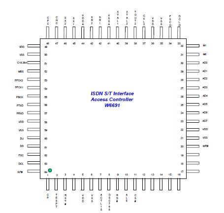
Pinout

  Connection Diagram


Description

W6691 consists of one D channel HDLC controller and two B HDLC controller channel access. The HDLC controller facilitates efficient access to signaling, data and voice services. It provides multiplex/non- mutiplexe 8- bit microprocessor interface. The interface is selected by external MBS selection. In addition, W6691 can be operated in TE, LT-S and LT-T mode programmed by external pin. In TE mode, W6691 provides PCM bus or GCI bus to connect with CODEC. In LT mode, it can used in NT2 application. W6691 also provides various B channel switching function among PCM, GCI and Layer2. It adopts 3.3V process to manufacture. The FIFO size of D channel is 64 byte. The FIFO size of two B channel are 128bytes. Two extended external interrupt is designed for peripheral interrupt saving extra interrupt circuit design. One layer activation indication output can be programmed by microprocessor control or W6691 chip internal control. The DPLL circuit is design in chip to generate the DCL and FSC signal for NT2 application. It can eliminate extra DPLL circuit on board. In order to save a lot of crystal on board, W6691 can provide 7.68MHz OSC signal for other chip needs the clock in TE or NT2 application.


Customers Who Bought This Item Also Bought

Margin,quality,low-cost products with low minimum orders. Secure your online payments with SeekIC Buyer Protection.
Power Supplies - External/Internal (Off-Board)
Connectors, Interconnects
Semiconductor Modules
Memory Cards, Modules
Test Equipment
Batteries, Chargers, Holders
View more