Features: • Guaranteed to meet full electrical specifications over TJ = 40°C to +125°C
• Second generation ASIC replacement technology
- Densities as high as 15,552 logic cells with up to 600,000 system gates
- Streamlined features based on Virtex-E architecture
- Unlimited in-system reprogrammability
- Very low cost
• System level features
- SelectRAM+™ hierarchical memory:
` 16 bits/LUT distributed RAM
` Configurable 4K-bit true dual-port block RAM
` Fast interfaces to external RAM
- Low-power segmented routing architecture
- Dedicated carry logic for high-speed arithmetic
- Efficient multiplier support
- Cascade chain for wide-input functions
- Abundant registers/latches with enable, set, reset
- Four dedicated DLLs for advanced clock control
` Eliminate clock distribution delay
` Multiply, divide, or phase shift
- Four primary low-skew global clock distribution nets
- IEEE 1149.1 compatible boundary scan logic
• Versatile I/O and packaging
- Low cost packages available in all densities
- Family footprint compatibility in common packages
- 19 high-performance interface standards
` LVTTL, LVCMOS, HSTL, SSTL, AGP, CTT, GTL
` LVDS and LVPECL differential I/O
- Up to 120 differential I/O pairs that can be input, output, or bidirectional
• Fully supported by powerful Xilinx ISE development system
- Fully automatic mapping, placement, and routing
- Integrated with design entry and verification tools
- Extensive IP library including DSP functions and soft
Specifications
| Symbol |
Description |
Min |
Max |
Units |
| VCCINT |
Supply voltage relative to GND |
0.5 |
2.0 |
V |
| VCCO |
Supply voltage relative to GND |
0.5 |
4.0 |
V |
| VREF |
Input reference voltage |
0.5 |
4.0 |
V |
| VIN |
Input voltage relative to GND(2,3) |
0.5 |
4.05 |
V |
| VTS |
Voltage applied to 3-state output (3) |
0.5 |
4.0 |
V |
| TSTG |
Storage temperature (ambient) |
65 |
+150 |
°C |
| TJ |
Junction temperature |
|
+135 |
°C |
Notes:
1. Stresses beyond those listed under Absolute Maximum Ratings may cause permanent damage to the device. These are stress ratings only, and functional operation of the device at these or any other conditions beyond those listed under Operating Conditions is not implied. Exposure to
Absolute Maximum Ratings conditions for extended periods of time may affect device reliability.
2. VIN should not exceed VCCO by more than 3.6V over extended periods of time (e.g., longer than a day).
3. Maximum DC overshoot must be limited to either VCCO + 0.5V or 10 mA, and undershoot must be limited to 0.5V or 10 mA, whichever is easier to achieve. The Maximum AC conditions are as follows: The device pins may undershoot to 2.0V or overshoot to VCCO + 2.0V, provided this over/undershoot lasts no more than 11 ns with a forcing current no greater than 100 mA.
4. For soldering guidelines, see the Packaging Information on the Xilinx Web site.
DescriptionThe Spartan™-IIE 1.8V Field-Programmable Gate Array family gives users high performance, abundant logic resources, and a rich feature set, all at an exceptionally low price. The seven-member family offers densities ranging from 50,000 to 600,000 system gates, as shown in Table 1. System performance is supported beyond 200 MHz.
Spartan-IIE devices deliver more gates, I/Os, and features per dollar than other FPGAs by combining advanced process technology with a streamlined architecture based on the proven Virtex™-E platform. Features include block RAM (to 288K bits), distributed RAM (to 221,184 bits), 19 selectable I/O standards, and four DLLs (Delay-Locked Loops). Fast, predictable interconnect means that successive design iterations continue to meet timing requirements.
The Spartan-IIE family is a superior alternative to mask-programmed ASICs. The FPGA avoids the initial cost, lengthy development cycles, and inherent risk of conventional ASICs. Also, FPGA programmability permits design upgrades in the field with no hardware replacement necessary (impossible with ASICs).

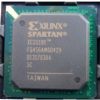
 XC2S300E Data Sheet