XC2V1000

Features: • Industry First Platform FPGA Solution• IP-Immersion Architecture- Densities from 40K to 8M system gates- 420 MHz internal clock speed (Advance Data)- 840+ Mb/s I/O (Advance Data)• SelectRAM™ Memory Hierarchy- 3 Mb of dual-port RAM in 18 Kbit block SelectRAM reso...

product image

XC2V1000 Picture
SeekIC No. : 004547809 Detail

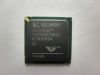
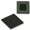
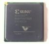
XC2V1000: Features: • Industry First Platform FPGA Solution• IP-Immersion Architecture- Densities from 40K to 8M system gates- 420 MHz internal clock speed (Advance Data)- 840+ Mb/s I/O (Advance D...

floor Price/Ceiling Price

Part Number:
XC2V1000
Supply Ability:
5000

Price Break

  • Qty
  • 1~5000
  • Unit Price
  • Negotiable
  • Processing time
  • 15 Days
Total Cost: $ 0.00

SeekIC Buyer Protection PLUS - newly updated for 2013!

  • Escrow Protection.
  • Guaranteed refunds.
  • Secure payments.
  • Learn more >>

Month Sales

268 Transactions

Rating

evaluate  (4.8 stars)

Upload time: 2024/4/18

Payment Methods

All payment methods are secure and covered by SeekIC Buyer Protection PLUS.

Notice: When you place an order, your payment is made to SeekIC and not to your seller. SeekIC only pays the seller after confirming you have received your order. We will also never share your payment details with your seller.
Product Details

Description


Features:

• Industry First Platform FPGA Solution
• IP-Immersion Architecture
- Densities from 40K to 8M system gates
- 420 MHz internal clock speed (Advance Data)
- 840+ Mb/s I/O (Advance Data)
• SelectRAM™ Memory Hierarchy
- 3 Mb of dual-port RAM in 18 Kbit block SelectRAM resources
- Up to 1.5 Mb of distributed SelectRAM resources
• High-Performance Interfaces to External Memory
- DRAM interfaces
· SDR / DDR SDRAM
· Network FCRAM
· Reduced Latency DRAM
- SRAM interfaces
· SDR / DDR SRAM
· QDR™ SRAM
- CAM interfaces
• Arithmetic Functions
- Dedicated 18-bit x 18-bit multiplier blocks
- Fast look-ahead carry logic chains
• Flexible Logic Resources
- Up to 93,184 internal registers / latches with Clock Enable
- Up to 93,184 look-up tables (LUTs) or cascadable
16-bit shift registers
- Wide multiplexers and wide-input function support
- Horizontal cascade chain and sum-of-products support
- Internal 3-state bussing
• High-Performance Clock Management Circuitry
- Up to 12 DCM (Digital Clock Manager) modules
· Precise clock de-skew
· Flexible frequency synthesis
· High-resolution phase shifting
- 16 global clock multiplexer buffers
• Active Interconnect Technology
- Fourth generation segmented routing structure
- Predictable, fast routing delay, independent of fanout
• SelectIO™-Ultra Technology
- Up to 1,108 user I/Os
- 19 single-ended and six differential standards
- Programmable sink current (2 mA to 24 mA) per
- Digitally Controlled Impedance (DCI) I/O: on-chip termination resistors for single-ended I/O standards
- PCI-X compatible (133 MHz and 66 MHz) at 3.3V
- PCI compliant (66 MHz and 33 MHz) at 3.3V
- CardBus compliant (33 MHz) at 3.3V
- Differential Signaling
· 840 Mb/s Low-Voltage Differential Signaling I/O (LVDS) with current mode drivers
· Bus LVDS I/O
· Lightning Data Transport (LDT) I/O with current driver buffers
· Low-Voltage Positive Emitter-Coupled Logic (LVPECL) I/O
· Built-in DDR input and output registers
- Proprietary high-performance SelectLink Technology
· High-bandwidth data path
· Double Data Rate (DDR) link
· Web-based HDL generation methodology
• Supported by Xilinx Foundation™ and Alliance Series™ Development Systems
- Integrated VHDL and Verilog design flows
- Compilation of 10M system gates designs
- Internet Team Design (ITD) tool
• SRAM-Based In-System Configuration
- Fast SelectMAP configuration
- Triple Data Encryption Standard (DES) security option (Bitstream Encryption)
- IEEE 1532 support
- Partial reconfiguration
- Unlimited reprogrammability
- Readback capability
• 0.15 µm 8-Layer Metal Process with 0.12 µm High-Speed Transistors
• 1.5V (VCCINT) Core Power Supply, Dedicated 3.3V VCCAUX Auxiliary and VCCO I/O Power Supplies
• IEEE 1149.1 Compatible Boundary-Scan Logic Support
• Flip-Chip and Wire-Bond Ball Grid Array (BGA) Packages in Three Standard Fine Pitches (0.80 mm, 1.00 mm, and 1.27 mm)
• 100% Factory Tested


Specifications

Symbol Description
Conditions
Units
VCCINT

VCCAUX

VCCO

VBATT

VREF

VIN(3)

VTS

TSTG

TSOL

TJ
Internal supply voltage relative to GND

Auxiliary supply voltage relative to GND

Output drivers supply voltage relative to GND

Key memory battery backup supply

Input reference voltage

Input voltage relative to GND (user and dedicated I/Os)

Voltage applied to 3-state output (user and dedicated I/Os)

Storage temperature (ambient)

Maximum soldering temp.

Operating junction temperature (2)
0.5 to 1.65

0.5 to 4.0

0.5 to 4.0

0.5 to 4.0

0.5 to VCCO + 0.5

0.5 to VCCO + 0.5

0.5 to 4.0

65 to +150

+220

+125
V

V

V

V

V

V

V

°C

°C

°C

Notes:
1. Stresses beyond those listed under Absolute Maximum Ratings might cause permanent damage to the device. These are stress ratings only, and functional operation of the device at these or any other conditions beyond those listed under Operating Conditions is not implied. Exposure to Absolute Maximum Ratings conditions for extended periods of time might affect device reliability.
2. For soldering guidelines and thermal considerations, see the Device Packaging information on the Xilinx website.
3. Inputs configured as PCI are fully PCI compliant. This statement takes precedence over any specification that would imply that the device is not PCI compliant.


Description

The Virtex-II family is a platform FPGA developed for high performance from low-density to high-density designs that are based on IP cores and customized modules.

The Virtex-II  family delivers complete solutions for telecommunication, wireless, networking, video, and DSP applications, including PCI, LVDS, and DDR interfaces. The leading-edge 0.15 µm / 0.12 µm CMOS 8-layer metal process and the Virtex-II architecture are optimized for high speed with low power consumption. Combining a wide variety of flexible features and a large range of densities up to 10 million system gates, the Virtex-II family enhances programmable logic design capabilities and is a powerful alternative to mask-programmed gates arrays. As shown in Table 1, the Virtex-II family comprises 11 members, ranging from 40K to 8M system gates.


Customers Who Bought This Item Also Bought

Margin,quality,low-cost products with low minimum orders. Secure your online payments with SeekIC Buyer Protection.
Industrial Controls, Meters
Memory Cards, Modules
Cables, Wires
Computers, Office - Components, Accessories
RF and RFID
Power Supplies - External/Internal (Off-Board)
View more