YGV619

Features: `Display planes: External digital image is overlaid with OSD images composed of regions.-Up to four planes, which are individually composed of back drop plane (plane on which external images areinputted)+ region, are available.` OSD image format:-8bit/dot palette mode, and 16 bit RGB or ...

product image

YGV619 Picture
SeekIC No. : 004549932 Detail

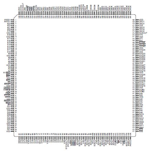
YGV619: Features: `Display planes: External digital image is overlaid with OSD images composed of regions.-Up to four planes, which are individually composed of back drop plane (plane on which external imag...

floor Price/Ceiling Price

Part Number:
YGV619
Supply Ability:
5000

Price Break

  • Qty
  • 1~5000
  • Unit Price
  • Negotiable
  • Processing time
  • 15 Days
Total Cost: $ 0.00

SeekIC Buyer Protection PLUS - newly updated for 2013!

  • Escrow Protection.
  • Guaranteed refunds.
  • Secure payments.
  • Learn more >>

Month Sales

268 Transactions

Rating

evaluate  (4.8 stars)

Upload time: 2024/4/15

Payment Methods

All payment methods are secure and covered by SeekIC Buyer Protection PLUS.

Notice: When you place an order, your payment is made to SeekIC and not to your seller. SeekIC only pays the seller after confirming you have received your order. We will also never share your payment details with your seller.
Product Details

Description


Features:

`Display planes: External digital image is overlaid with OSD images composed of regions.
-Up to four planes, which are individually composed of back drop plane (plane on which external images areinputted)+ region, are available.
` OSD image format:
-8bit/dot palette mode, and 16 bit RGB or YCbCr format can be selected.
-YCbCr conforms to the conversion method of ITU601.
-Color palette (256 colors in 16777 k colors) can be specified by region.
`Digital image input format:
-18bitR6G6B6 (Max. dot clock frequency: 80 MHz)
-16bitYCbCr422 (Max. dot clock frequency: 80 MHz)
-8bitITU656 (Dot clock frequency 27 MHz)
` Digital image output format:
- R6G6B6 + 2 bit AT
-18bitYCbCr444 + 2 bit AT
-16bitYCbCr422 + 2 bit AT
-8bitITU656 + 2 bit AT + 6 bit a blending coefficient
`Max. OSD resolution: 960 dots * 1080 lines
-(However, max. resolution of overlaid external image is 1920 *1080 lines)
`Applicable digital TV image format:
-525i
-525p
-1125i
`Video capture function:
-Draws external image input on the frame memory in real time.
-Can convert resolution.
-Provided with progressive scanning conversion
` Priority of display planes
- Regular priority: Plane D > Plane C > Plane B > Plane A > Back drop plane
-The priority can be changed by region.
` a blending function (64 intensity level)
-Blending weight can be set by dot.
` Flicker cancel filter is built in.Enabling / disabling flicker cancel function can be set by region.
`8 bit DACs are built in for R, G and B individually. (Max. operating frequency: 80 MHz)
` Two PLLs are built in. (1: Generates SDRAM clock and system clock 2: Generates dot clock)
` Display monitor control
-Display resolution and scanning frequency can be set optionally.This function is compatible with progressive scanning and interlaced scanning modes.NTSC subcarrier output
`SDRAM can be added externally as VRAM (SDRAM generation clock frequency: Max. 80 MHz.)
-16 bit bus 512k words * 16 bits * 2 banks * 1 pc. (capacity: 2M bytes)1M words * 16 bits * 4 banks * 1 pc. (capacity: 8M bytes) 2M words * 16 bits * 2 banks * 1 pc. (capacity: 8M bytes)
32 bit bus
-512k words * 16 bits * 2 banks * 2 pcs. (capacity: 4M bytes)
-512k words * 32 bits * 4 banks * 1 pc. (capacity: 8M bytes)
-1M words * 16 bits * 4 banks * 2 pcs. (capacity: 16M bytes)
-2M words * 16 bits * 2 banks * 2 pcs. (capacity: 16M bytes)
` CPU interface
-Compatible with 16/32 bit CPU. Various built-in tables can be mapped on CPU space.
-Compatible with little endian and big endian
` Package: 240SQFP (YGV619-S)
` Operating temperature range: -45 to +85
` Power supply: 3.3V, single power supply


Pinout

  Connection Diagram


Specifications

Items
Symbol
Ratings
Unit
Supply Voltage
VDD*1
-0.5 to +4.6
V
Input Voltage*2
VI*1
-0.5 to VDD+ 0.5
V
Input Voltage*3
VI*1
-0.5 to 5.5
V
Output Voltage*2
VO*1
-0.5 to VDD+ 0.5
V
Output Current
IO
-20 to +20
mA
Storage temperature
Tstg
-50 to +125
*1: Value with respect to VSS (GND) = 0V
*2: for no-tolerant pins
*3: for tolerant pins


Customers Who Bought This Item Also Bought

Margin,quality,low-cost products with low minimum orders. Secure your online payments with SeekIC Buyer Protection.
Semiconductor Modules
Line Protection, Backups
Computers, Office - Components, Accessories
Crystals and Oscillators
Hardware, Fasteners, Accessories
View more