Features: • Common Latch-Enable Control
• Common Three-State Output Enable Control
• Buffered Inputs
• Three-State Outputs
• Bus Line Driving Capacity
• Typical Propagation Delay = 13ns at VCC = 5V,
CL = 15pF, TA = 25oC (Data to Output)
• Fanout (Over Temperature Range)
- Standard Outputs . . . . . . . . . . . . . . . 10 LSTTL Loads
- Bus Driver Outputs . . . . . . . . . . . . . 15 LSTTL Loads
• Wide Operating Temperature Range . . . -55oC to 125oC
• Balanced Propagation Delay and Transition Times
• Significant Power Reduction Compared to LSTTL Logic ICs
• HC Types
- 2V to 6V Operation
- High Noise Immunity: NIL = 30%, NIH = 30% of VCC at VCC = 5V
• HCT Types
- 4.5V to 5.5V Operation
- Direct LSTTL Input Logic Compatibility,
VIL= 0.8V (Max), VIH = 2V (Min)
- CMOS Input Compatibility, Il 1mA at VOL, VOH
Pinout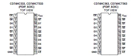 Specifications
DC Supply Voltage, VCC . . . . . . . . . . . . . . . . .. -0.5V to 7V
DC Input Diode Current, IIK
For VI < -0.5V or VI > VCC + 0.5V . . . . . . . . . . . . .±20mA
DC Output Diode Current, IOK
For VO < -0.5V or VO > VCC + 0.5V . . . . . . . . . . . .±20mA
DC Drain Current, per Output, IO
For -0.5V < VO < VCC + 0.5V. . . . . . . . . . . . . . . . .±35mA
DC Output Source or Sink Current per Output Pin, IO
For VO > -0.5V or VO < VCC + 0.5V . . . . . . . . . . . .±25mA
DC VCC or Ground Current, ICC . . . . . . . . . . . . . .±50mA
Operating Conditions
Temperature Range, TA . . . . . . . . . . . . .. -55oC to 125oC
Supply Voltage Range, VCC
HC Types . . . . . . . . . . . . . . . . . . . . . . . . . . . .. . .2V to 6V
HCT Types . . . . . . . . . . . . . . . . . . . . . . . . . .4.5V to 5.5V
DC Input or Output Voltage, VI, VO . . . . . . . . . 0V to VCC
Input Rise and Fall Time
2V . . . . . . . . . . . . . . . . . . . . . . . . . . . . . . . 1000ns (Max)
4.5V. . . . . . . . . . . . . . . . . . . . . . . . . . . . . . . 500ns (Max)
6V . . . . . . . . . . . . . . . . . . . . . . . . . . . . . . . . 400ns (Max)
Thermal Resistance (Typical, Note 3) JA (oC/W)
PDIP Package . . . . . . . . . . . . . . . . . . . . . . . . . . . . . 125
SOIC Package . . . . . . . . . . . . . . . . . . . . . . . . . . . . . 120
Maximum Junction Temperature . . . . . . . . . . . . . 150oC
Maximum Storage Temperature Range . .-65oC to 150oC
Maximum Lead Temperature (Soldering 10s) . . . . 300oC
(SOIC - Lead Tips Only)
CAUTION: Stresses above those listed in "Absolute Maximum Ratings" may cause permanent damage to the device. This is a stress only rating and operation of the device at these or any other conditions above those indicated in the operational sections of this specification is not implied.
NOTE:
3. JA is measured with the component mounted on an evaluation PC board in free air.
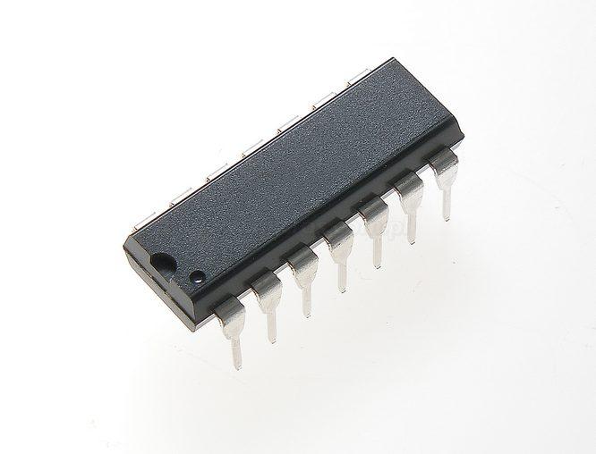
DescriptionThe Harris CD74HC533, CD74HCT533, CD74HC563, and CD74HCT563 are high speed Octal Transparent Latches manufactured with silicon gate CMOS technology. They possess the low power consumption of standard CMOS integrated circuits, as well as the ability to drive 15 LSTTL devices.
CD74HCT563 outputs are transparent to the inputs when the latch enable (LE) is high. When the latch enable (LE) goes low the data is latched. The output enable (OE) controls the threestate outputs. When the output enable (OE) is high the outputs are in the high impedance state. The latch operation is independent to the state of the output enable.
The CD74HC533 and CD74HCT533 are identical in function to the CD74HC563 and CD74HCT563 but have different pinouts. The CD74HC533 and CD74HCT533 are similar to the CD74HC373 and CD74HCT373; the latter are noninverting types.

 CD74HCT563 Data Sheet