Pinout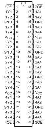 SpecificationsSupply voltage range, V CC . . . . . . . . . . . . . . . . . . . . . . . . . . . . . . . . . . . . . . . . . 0.5 V to 4.6 V
Input voltage range, V I(see Note 1) . . . . . . . . . . . . . . . . . . . . . . . . . . . . . . . . . . 0.5 V to 7 V
Voltage range applied to any output in the high-impedance
or power-off state, V O (see Note 1) . . . . . . . . . . . . . . . . . . . . . . . . . . . . . . . . . . . 0.5 V to 7 V
Voltage range applied to any output in the high state, V O (see Note 1) . .0.5 V to VCC + 0.5 V
Current into any output in the low state, I O : SN54LVT16244B . . . . . . . . . . . . . . .. . . . . 96 mA
SN74LVT16244B . . . . . . . . . . . . . . . . . . . . . . . . . . . . . . . . 128 mA
Current into any output in the high state, I O (see Note 2): SN54LVT16244B . .. .. . . . . . 48 mA
SN74LVT16244B . . . . . . . . . . . . . . . . . . . . . . . . . . . . . . . . . . . . . . . . . . . . . . . . . . . .. . . . . . 64 mA
Input clamp current, I IK (V 1< 0) . . . . . . . . . . . . . . . . . . . . . . . . . . . . . . . . . . . . . . . . . . 50 mA
Output clamp current, I OK (V O< 0) . . . . . . . . . . . . . . . . . . . . . . .. . . . . . . . . . . . . . . . . . 50 mA
Package thermal impedance, q JA (see Note 3): DGG package . . . . . . . . .. . . . . . . . . . 70°C/W
DGV package . . . . . . . . . . . . . . . . . . . . . . . . . . . . . . . . . . . . . . . . . . . . . . . . . . . . 58°C/W
DL package . . . . . . . . . . . . . . . . . . . . . . . . . . . . . . . . . . . . . . . . . . . . . . . . . . . . . 63°C/W
Storage temperature range, T stg . . . . . . . . . . . . . . . . . . . . . . . . . . .. . . . . . . . . . 65 to 150 DescriptionThe SN74LVT16244B devices are 16-bit buffers and line drivers designed for low-voltage (3.3-V) V
CC operation, but with the capability to provide a TTL interface to a 5-V system environment. These devices can be used as four 4-bit buffers, two 8-bit buffers, or one 16-bit buffer. These devices provide true outputs and symmetrical active-low output-enable (OE) inputs.
When V
CC is between 0 and 1.5-V, the devices SN74LVT16244B are in the high-impedance state during power up or power down. However, to ensure the high-impedance state above 1.5-V, OE should be tied to V
CC through a pullup resistor; the minimum value of the resistor is determined by the current-sinking capability of the driver.
These devices are fully specified for hot-insertion applications using I and power-up 3-state. The I circuitry off off disables the outputs, preventing damaging current backflow through the devices when they are powered down.The power-up 3-state circuitry places the outputs in the high-impedance state during power up and power down, which prevents driver conflict.
The SN54LVT16244B is characterized for operation over the full military temperature range of 55°C to 125°C. The SN74LVT16244B is characterized for operation from 40°C to 85°C.

 SN74LVT16244B Data Sheet


