Features: 10MHz to 320MHz Input/Output Operation
Low Output to Output Skew (<50ps)
Low Jitter Peak-to-Peak(<70ps)
Up to 20 Programmable Fan-out Buffers
• Programmable output standards and individual enable controls
- LVTTL, LVCMOS, HSTL, SSTL, LVDS, LVPECL
• Programmable precision output impedance
- 40 to 70Ω in 5Ω increments
• Programmable slew rate
• Up to 10 banks with individual V CCO and GND
- 1.5V, 1.8V, 2.5V, 3.3V
Fully Integrated High-Performance PLL
• Programmable lock detect
• Multiply and divide ratio controlled by
- Input divider (5 bits)
- Internal feedback divider (5 bits)
- Five output dividers (5 bits)
• Programmable On-chip Loop Filter
Precision Programmable Phase Adjustment (Skew) Per Output
• 16 settings; minimum step size 195ps
- Locked to VCO frequency
• Up to +/- 12ns skew range
• Coarse and fine adjustment modes
Up to Five Clock Frequency Domains
Flexible Clock Reference Inputs
• Programmable input standards
- LVTTL, LVCMOS, SSTL, HSTL, LVDS, LVPECL
• Clock A/B selection multiplexer
• Programmable precision termination
Four User-programmable Profiles Stored in E2CMOS® Memory
• Supports both test and multiple operating configurations
Full JTAG Boundary Scan Test In-System Programming Support
Exceptional Power Supply Noise Immunity
Commercial (0 to 70) and Industrial (-40 to 85) Temperature Ranges
100-pin and 48-pin TQFP Packages
Application• Circuit board common clock generation and distribution
• PLL-based frequency generation
• High fan-out clock bufferPinout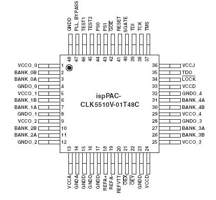
SpecificationsCore Supply Voltage VCCD. . . . . . . . . . . . . . . . . . . . . . . . . . . . . . . . -0.5 to 5.5V
PLL Supply Voltage VCCA. . . . . . . . . . . . . . . . . . . . . . . . . . . . . . . . . -0.5 to 5.5V
JTAG Supply Voltage VCCJ. . . . . . . . . . . . . . . . . . . . . . . . . . . . . . . . -0.5 to 5.5V
Output Driver Supply Voltage VCCO. . . . . . . . . . . . . . . . . . . . . . . . . -0.5 to 4.5V
Input Voltage . . . . . . . . . . . . . . . . . . . . . . . . . . . . . . . . . . . . . . .. . . -0.5 to 4.5V
Output Voltage1. . . . . . . . . . . . . . . . . . . . . . . . . . . . . . . . . . . . . . . . -0.5 to 4.5V
Storage Temperature . . . . . . . . . . . . . . . . . . . . . . . . . . . . .. . . . . . . -65 to 150
Junction Temperature with power supplied . . . . . . . . . . . . . . . . . . . -40 to 130DescriptionThe ispClock5510 and ispClock5520 are in-system-programmable high-fanout PLL-based clock drivers designed for use in high performance communications and computing applications. The ispClock5510 provides up to 10 single- ended or five differential clock outputs, while the ispClock5520 provides up to 20 single-ended or 10 differential clock outputs. Each pair of outputs may be independently configured to support separate I/O standards (LVDS, LVPECL, LVTTL, LVCMOS, SSTL, HSTL) and output frequency. In addition, each output provides independent programmable control of termination, slew-rate, and timing skew. All configuration information is stored on-chip in nonvolatile E2CMOS memory.
The ispClock5500's PLL and divider systems supports the synthesis of clock frequencies differing from that of the reference input through the provision of programmable input and feedback dividers. A set of five post-PLL V-dividers provides additional flexibility by supporting the generation of five separate output frequencies. Loop feedback may be taken from the output of any of the five V-dividers.
The core functions of all members of the ispClock5500 family are identical, the differences between devices being restricted to the number of inputs and outputs, as shown in the following table.

 ispClock5510 Data Sheet


