Want to post a buying lead? If you are not a member yet, please select the specific/related part number first and then fill the quantity and your contact details in the "Request for Quotation Form" on the left, and then click "Send RFQ".Your buying lead can then be posted, and the reliable suppliers will quote via our online message system or other channels soon.
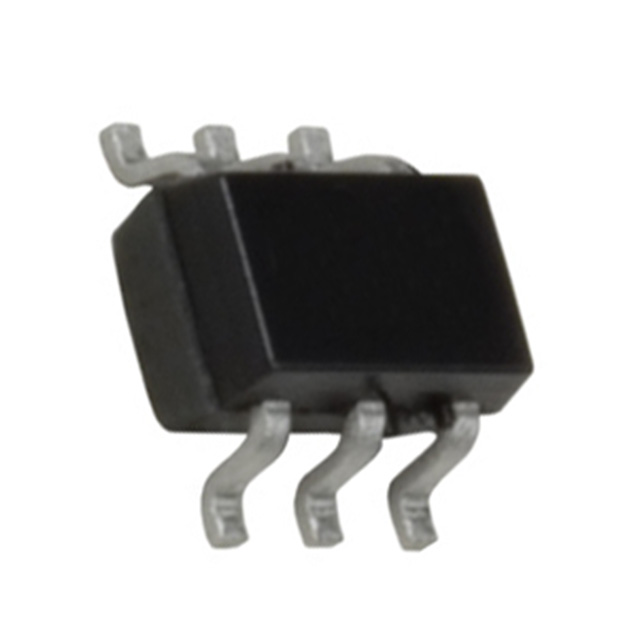
This device is particularly suited for compact powermanagement in portable electronic equipment where2.5V to 8V input and 0.8A output current capability areneeded. This load switch integrates a small N-Channelpower MOSFET (Q1) that drives a large P-Channelpower MOSFET (Q2) in one tiny SC70-6 package.
FDG6331L Maximum Ratings
Product
Product status
Eco Status
Pricing*
Package type
Leads
Packing method
Package Drawing
Package Marking Convention**
FDG6331L
Full Production
RoHS Compliant
$0.204
SC70-6
6
TAPE REEL
Line 1: &Y (Binary Calendar Year Coding) Line 2: .31
* Fairchild 1,000 piece Budgetary Pricing
** A sample button will appear if the part is available through Fairchild's on-line samples program. If there is no sample button, please contact a Fairchild distributor to obtain samples
Package marking information for product FDG6331L is available. Click here for more information .
FDG6331L Features
• 0.8 A, 8 V. RDS(ON) = 260 mΩ @ VGS = 4.5 V RDS(ON) = 330 mΩ @ VGS = 2.5 V RDS(ON) = 450 mΩ @ VGS = 1.8 V • Control MOSFET (Q1) includes Zener protection for ESD ruggedness (>6KV Human body model) • High performance trench technology for extremely low RDS(ON) • Compact industry standard SC70-6 surface mount package
The N & P-Channel MOSFETs are produced using Fairchild Semiconductor's advanced PowerTrench process that has been especially tailored to minimize on-state resistance and yet maintain superior switching performance.
These devices have been designed to offer exceptional power dissipation in a very small footprint for applications where the bigger more expensive TSSOP-8 and SSOP-6 packages are impractical.
FDG6332C Maximum Ratings
Symbol
Parameter
Q1
Q2
Units
VDSS VGSS
Drain-Source Voltage Gate-Source Voltage
20 ±12 0.7 2.1
20 ±12 0.6 2
V V A
W
°C
ID
Drain Current Continuous Pulsed
(Note 1)
PD
Power Dissipation for Single Operation
(Note 1)
0.3 55 to +150
TJ,TSTG
Operating and Storage Junction Temperature Range
FDG6332C Features
` Q1 0.7 A, 20V. RDS(ON) = 300 mW @ VGS = 4.5 V RDS(ON) = 400 mW @ VGS = 2.5 V ` Q2 0.6 A, 20V. RDS(ON) = 420 mW @ VGS = 4.5 V RDS(ON) = 630 mW @ VGS = 2.5 V ` Low gate charge ` High performance trench technology for extremely low RDS(ON) ` SC70-6 package: small footprint (51% smaller than SSOT-6); low profile (1mm thick)