Want to post a buying lead? If you are not a member yet, please select the specific/related part number first and then fill the quantity and your contact details in the "Request for Quotation Form" on the left, and then click "Send RFQ".Your buying lead can then be posted, and the reliable suppliers will quote via our online message system or other channels soon.
This Digital Audio HEXFET® is specifically designed for Class-D audio amplifier applications. This MosFET utilizes the latest processing techniques to achieve low on-resistance per silicon area. Furthermore, Gate charge, body-diode reverse recovery and internal Gate resistance are optimized to improve key Class-D audio amplifier performance factors such as efficiency, THD and EMI. Additional features of this MosFET are 175 operating junction temperature and repetitive avalanche capability. These features combine to make this MosFET a highly efficient, robust and reliable device for Class-D audio amplifier applications.
IRLIB4343PBF Maximum Ratings
Symbol
Parameter
Max.
Units
VDS
Drain-Source Voltage
55
V
VGS
Gate-to-Source Voltage
±20
ID @ TC = 25
Continuous Drain Current, VGS @ 10V
19
A
ID @ TC= 100
Continuous Drain Current, VGS @ 10V
13
IDM
Pulsed Drain Current1
80
PD @TC = 25
Power Dissipation
39
W
PD @TC = 100
Power Dissipation
20
Linear Derating Factor
0.26
W/
TJ
Operating Junction and
-40 to + 175
TSTG
Storage Temperature Range
Mounting torque, 6-32 or M3 screw
10lb`in (1.1N`m)
IRLIB4343PBF Features
Advanced Process Technology Key Parameters Optimized for Class-D Audio Amplifier Applications Low RDSON for Improved Efficiency Low Qg and Qsw for Better THD and Improved Efficiency Low Qrr for Better THD and Lower EMI 175 Operating Junction Temperature for Ruggedness Repetitive Avalanche Capability for Robustness and Reliability Lead-Free
IRLIB9343 General Description
This Digital Audio HEXFET® is specifically designed for Class-D audio amplifier applications. This MosFET utilizes the latest processing techniques to achieve low on-resistance per silicon area. Furthermore, Gate charge, body-diode reverse recovery and internal Gate resistance are optimized to improve key Class-D audio amplifier performance factors such as efficiency, THD and EMI. Additional features of this MosFET are 175°C operating junction temperature and repetitive avalanche capability.
These features combine to make this MosFET a highly efficient, robust and reliable device for Class-D audio amplifier applications.
IRLIB9343 Maximum Ratings
Parameter
Max.
Units
VDS
Drain-to-Source Voltage
-55
V
VGS
Gate-to-Source Voltage
±20
ID @TC = 25°C
Continuous Drain Current, VGS @ -10V
-14
A
ID @TC = 100°C
Continuous Drain Current, VGS @ -10V
-10
IDM
Pulsed Collector Current
-60
PD @TC = 25°C
Power Dissipation
33
W
PD @TC =100°C
Power Dissipation
20
Linear Derating Factor
0.26
°C
TJ TSTG
Operating Junction and Storage Temperature Range
-40 to + 175
Mounting Torque, 6-32 or M3 Screw
10 lbf•in (1.1 N•m)
IRLIB9343 Features
· Advanced Process Technology · Key Parameters Optimized for Class-D Audio Amplifier Applications · Low RDSON for Improved Efficiency · Low Qg and Qsw for Better THD and Improved Efficiency · Low Qrr for Better THD and Lower EMI · 175°C Operating Junction Temperature for Ruggedness · Repetitive Avalanche Capability for Robustness and Reliability
IRLIB9343PBF Parameters
Technical/Catalog Information
IRLIB9343PBF
Vendor
International Rectifier
Category
Discrete Semiconductor Products
Mounting Type
Through Hole
FET Polarity
P-Channel
Drain to Source Voltage (Vdss)
55V
Current - Continuous Drain (Id) @ 25° C
14A
Rds On (Max) @ Id, Vgs
105 mOhm @ 3.4A, 10V
Input Capacitance (Ciss) @ Vds
660pF @ 50V
Power - Max
33W
Packaging
Tube
Gate Charge (Qg) @ Vgs
47nC @ 10V
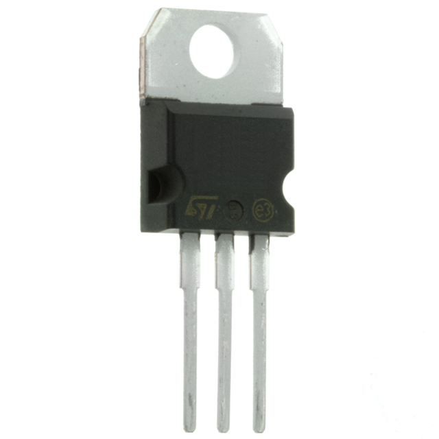
Package / Case
TO-220-3 Fullpak (Straight Leads)
FET Feature
Standard
Drawing Number
*
Lead Free Status
Lead Free
RoHS Status
RoHS Compliant
Other Names
IRLIB9343PBF IRLIB9343PBF
IRLIB9343PBF General Description
This Digital Audio HEXFET® is specifically designed for Class-D audio amplifier applications. This MosFET utilizes the latest processing techniques to achieve low on-resistance per silicon area. Furthermore, Gate charge, body-diode reverse recovery and internal Gate resistance are optimized to improve key Class-D audio amplifier performance factors such as efficiency, THD and EMI. Additional features of this MosFET are 175 operating junction temperature and repetitive avalanche capability.
These features combine to make this MosFET a highly efficient, robust and reliable device for Class-D audio amplifier applications.
IRLIB9343PBF Maximum Ratings
Symbol
Parameter
Max.
Units
VDS
Drain-Source Voltage
-55
V
VGS
Gate-to-Source Voltage
±20
ID @ TC = 25
Continuous Drain Current, VGS @ 10V
-14
A
ID @TC= 100
Continuous Drain Current, VGS @ 10V
-10
IDM
Pulsed Drain Current1
-60
PD @TC = 25
Power Dissipation
33
W
PD@TC = 100
Power Dissipation
20
Linear Derating Factor
0.26
W/
TJ
Operating Junction and
-40 to + 175
TSTG
Storage Temperature Range
Mounting torque, 6-32 or M3 screw
10 (1.1)
10lb`in (1.1N`m)
IRLIB9343PBF Features
Advanced Process Technology Key Parameters Optimized for Class-D Audio Amplifier Applications Low RDSON for Improved Efficiency Low Qg and Qsw for Better THD and Improved Efficiency Low Qrr for Better THD and Lower EMI 175 Operating Junction Temperature for Ruggedness Repetitive Avalanche Capability for Robustness and Reliability Lead-Free