Amplifier Circuit
Used for floating-point transform gain variable buffer amplifier circuit
Published:2011/8/31 1:14:00 Author:Jessie | Keyword: floating-point transform, gain variable, buffer amplifier | From:SeekIC
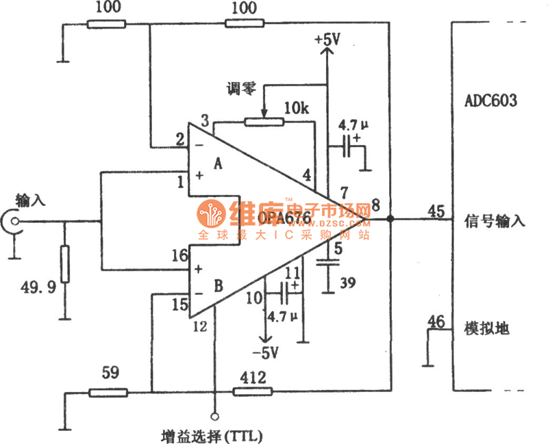
As shown in figure, the circuitis floating-point transform gain variable buffer amplifier circuit. The circuit consists of two parts: the buffer amplifier composedof OPA676 and theA/D conversion interface circuitcomposedof ADC603. OPA676 integrated chip's internal has two characteristics identical but independent differential amplification input levels. The two channels A and B can realize strobe by choosing pin 12's level. That is, when pins 12 is ata high level, channel A works, channel B cuts off; When pin 12 isat a low level, channel A cuts off, channel B works. The two channels' gains are different, using pin 12'scorresponding chose can realize gain's choice. We can learn from the diagram: Channel A voltage magnification is AVA=1+R2/R1=2; Channel B's voltage magnification is AvB=1+R4/R3=1+412/59=8.
Reprinted Url Of This Article:
http://www.seekic.com/circuit_diagram/Amplifier_Circuit/Used_for_floating_point_transform_gain_variable_buffer_amplifier_circuit.html
Print this Page | Comments | Reading(3)

Article Categories
power supply circuit
Amplifier Circuit
Basic Circuit
LED and Light Circuit
Sensor Circuit
Signal Processing
Electrical Equipment Circuit
Control Circuit
Remote Control Circuit
A/D-D/A Converter Circuit
Audio Circuit
Measuring and Test Circuit
Communication Circuit
Computer-Related Circuit
555 Circuit
Automotive Circuit
Repairing Circuit
Code: