Basic Circuit
4-20 mA Input and 5 V Output I/V Switching Circuit of LM324
Published:2011/8/1 22:23:00 Author:Michel | Keyword: 4-20 mA Input, 5 V Output, I/V Switching Circuit | From:SeekIC
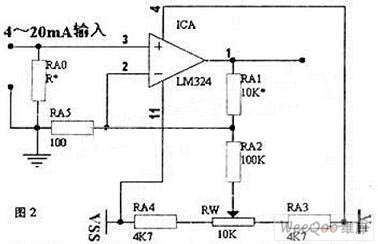
The simple way to solve the above problem is that the buffer processing circuit composed of operational amplifier is installed before singal chip inputs and it is showed as the picture.Increasing this level operation amplifier can make zero processing become easier and it will not cost SCM internal resources.Especially,when single chips uses A/D interface to receive the input of voltage whose zero signal is not zero,which ensures A/D conversion digits capital can be all used in the useful signal.
Take 4 ~ 20 mA for example, the RA0 of picture B is current sampling resistor, and its value is restricted by the sensor power supply voltage, when the current level uses 24 V power supply, RA0 often uses 500 Ω resistance when it is 24V power supply. The voltage is changed into 10V when it's 20mA.
Reprinted Url Of This Article:
http://www.seekic.com/circuit_diagram/Basic_Circuit/4_20_mA_Input_and_5_V_Output_I_V_Switching_Circuit_of_LM324.html
Print this Page | Comments | Reading(3)

Article Categories
power supply circuit
Amplifier Circuit
Basic Circuit
LED and Light Circuit
Sensor Circuit
Signal Processing
Electrical Equipment Circuit
Control Circuit
Remote Control Circuit
A/D-D/A Converter Circuit
Audio Circuit
Measuring and Test Circuit
Communication Circuit
Computer-Related Circuit
555 Circuit
Automotive Circuit
Repairing Circuit
Code: