Basic Circuit
Push pull circuit using complementary transistor and CMOS driving stage
Published:2011/4/19 22:38:00 Author:May | Keyword: Push pull, complementary transistor, CMOS driving stage | From:SeekIC
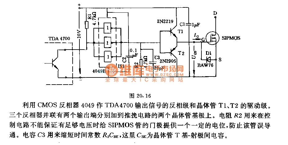
It is using CMOS inverter 4049 as driving stage of inverter stage of TDA4700 's output signal and transistor T1, T2. Three inverters are parallel. Two output ends among them are separately adding to the base of two transistors in push pull circuit. Resistor R2 is used for controlling the circuit. When it can not guarantee enough voltage for SIPMOS tube's gate pole to offer a fixed potential, it can prevent the error breaking over of this tube. Capacitor C3 is used for shorting time constant R2CBE. Here, CBE is capacitor between base-emitter of transistor T.
Reprinted Url Of This Article:
http://www.seekic.com/circuit_diagram/Basic_Circuit/Push_pull_circuit_using_complementary_transistor_and_CMOS_driving_stage.html
Print this Page | Comments | Reading(3)

Article Categories
power supply circuit
Amplifier Circuit
Basic Circuit
LED and Light Circuit
Sensor Circuit
Signal Processing
Electrical Equipment Circuit
Control Circuit
Remote Control Circuit
A/D-D/A Converter Circuit
Audio Circuit
Measuring and Test Circuit
Communication Circuit
Computer-Related Circuit
555 Circuit
Automotive Circuit
Repairing Circuit
Code: